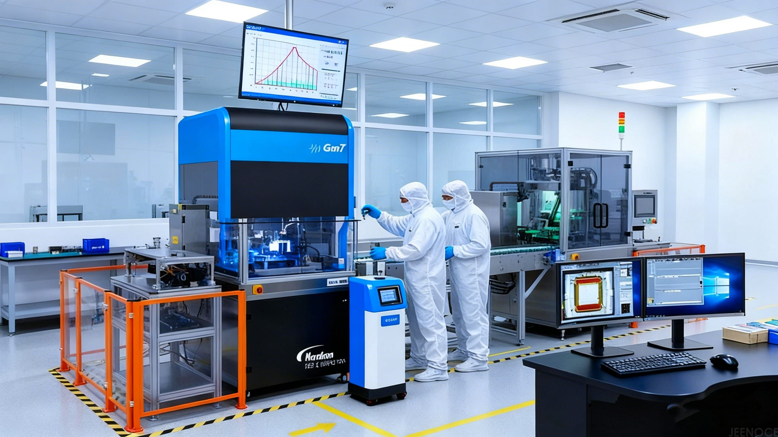
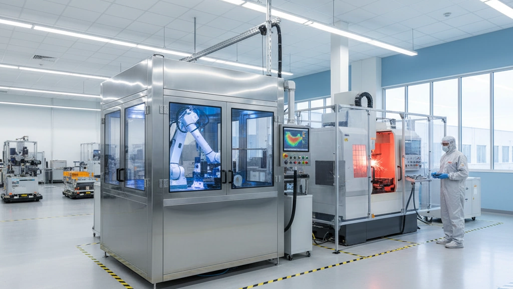
If you’re involved in smart manufacturing or electronics quality control, you already understand that tiny, unseen flaws can trigger costly failures. Did you know that undetected subsurface defects in SMT assemblies account for up to 30% of device malfunctions? That’s where scanning acoustic microscopy (SAM) becomes a game-changer. As a precise, non-destructive technique, SAM reveals internal voids, delaminations, and cracks invisible to traditional inspection methods. But mastering industry standards like JEDEC and IPC, while leveraging the latest technological advancements—from high-frequency imaging to AI-driven automation—is what truly sets manufacturers apart. In this post, we’ll uncover how meeting these SAM standards and innovations not only ensures reliability but also turbocharges your production lines—helping you stay ahead in a competitive market. Ready to dive in?
Scanning Acoustic Microscopy (SAM) has come a long way since its early days in the 1970s. Back then, it started as a proof-of-concept technology using basic ultrasonic transducers to image materials beneath surfaces. Fast forward to today, and we have powerful systems like C-mode Scanning Acoustic Microscopy (C-SAM) and high-resolution variants designed for precise, non-destructive evaluation in manufacturing and research.
Early SAM prototypes laid the foundation by demonstrating how focused sound waves could reveal hidden defects without damaging the sample. These initial devices were bulky and limited in resolution but proved ultrasonic non-destructive testing could detect subsurface voids and delamination effectively.
Today, modern C-SAM systems offer refined imaging capabilities. C-SAM scans samples in a single plane—known as the C-mode—producing detailed cross-sectional images of internal features. This evolution has unlocked widespread use in semiconductor inspection, electronics assembly, and material science.
At its core, SAM relies on focused ultrasonic transducers that emit high-frequency sound waves, typically in the MHz to low GHz range, into a sample. These waves interact with internal structures and reflect back or transmit through variations in acoustic impedance (basically, resistance to sound).
There are two main imaging modes:
Reflection mode: Captures echoes from internal interfaces, highlighting voids, cracks, or delamination.
Transmission mode: Measures waves passing through, useful for thin samples or detecting changes in thickness.
The contrast in SAM images arises from different acoustic impedances in the materials—think of it as how sound bounces differently off wood versus metal. This contrast helps pinpoint defects that are invisible to optical or X-ray methods.
Several SAM variants help target specific manufacturing needs:
C-SAM (C-mode Scanning Acoustic Microscopy): The most common type, ideal for non-destructive void and delamination analysis in semiconductor packages and solder joints.
CSAM: Another term often used interchangeably with C-SAM, emphasizing scanning and imaging quality.
SLAM (Scanning Laser Acoustic Microscopy): Combines laser technology for improved resolution and is gaining traction for advanced materials where traditional transducers struggle.
Each variant offers unique benefits:
C-SAM is perfect for inline quality control in Surface Mount Technology (SMT) assembly lines.
SLAM is valuable in research environments focusing on novel composites or semiconductor layers.
CSAM systems provide a good balance of speed and resolution for broad industrial applications.
Together, these technologies form the backbone of ultrasonic inspection, enabling manufacturers to catch subsurface faults early, reduce rework, and ensure product reliability.

Scanning Acoustic Microscopy (SAM) plays a crucial role in quality control, especially in electronics and semiconductor industries. To maintain reliability and consistency, several industry standards govern its use.
JEDEC standards cover semiconductor defect inspection, ensuring void analysis and delamination detection meet strict quality levels.
IPC standards, including IPC-A-610 (Acceptability of Electronic Assemblies) and J-STD-035 (Handling of Moisture Sensitive Devices), set the bar for manufacturing acceptability and moisture-related reliability.
MIL-STD-883 defines military-grade testing protocols, with emphasis on non-destructive evaluation like ultrasonic testing to guarantee high-reliability devices.
Beyond these, ASTM provides standardized SAM test procedures, helping users maintain uniform inspection methods. For aerospace and space applications, ESA guidelines demand rigorous space-grade reliability assessments, pushing SAM to detect even the smallest subsurface defects.
Calibration: Accurate SAM measurements require routine calibration of high-frequency transducers.
Sample Preparation: Surface finish and coupling mediums must be controlled to avoid false readings.
Automation Integration: Incorporating SAM into automated lines demands synchronization with robotics and data systems, which remains a complex task in many facilities.
Jeenoce has successfully integrated SAM inspections aligned with IPC standards into smart manufacturing lines, significantly reducing rework rates. By automating scanning and data analysis, Jeenoce solutions deliver consistent defect identification that matches industry benchmarks, enhancing both throughput and product reliability. You can explore how Jeenoce’s industry solutions optimize SAM applications for better compliance and efficiency.
This fusion of standardized inspection and smart automation sets a solid foundation for modern SAM usage, ensuring ultrasonic non-destructive testing meets today’s demanding industrial requirements.
Scanning Acoustic Microscopy (SAM) is rapidly evolving, with high-frequency breakthroughs leading the way. Modern systems now operate in the gigahertz range, enabling detection of defects smaller than 50 microns. This level of high-resolution SAM imaging is a game-changer for industries needing ultra-precise subsurface defect detection.
Alongside frequency advances, 3D and broadband SAM technologies have taken a big leap forward. Time-resolved reconstruction techniques combined with broadband transducers now deliver clearer, more detailed images—offering a fuller picture of material integrity through 3D acoustic tomography.
Automation and AI are also transforming SAM. AI-driven defect classification speeds up inspections while improving consistency, cutting down manual review time significantly. This shift makes inline quality control automation more practical, especially in fast-paced manufacturing environments.
Emerging modes like ultrasound impedance microscopy and nonlinear imaging techniques are expanding what SAM can do, revealing subtle material contrasts and hidden flaws traditional methods might miss.
Jeenoce is integrating these innovations into smart factory solutions, enabling real-time SAM data processing and automated decision-making on the production line. This seamless integration helps manufacturers achieve higher yields and lower rework rates. For more on these smart SAM automation workflows, Jeenoce offers detailed technical insights on their website.
Explore Jeenoce’s latest updates on cutting-edge scanning acoustic microscopy technologies and automation at Jeenoce Technical Insights.

Scanning acoustic microscopy (SAM) plays a crucial role in smart manufacturing, especially in semiconductor and electronics production. It detects voids, delamination, and incomplete underfill in surface-mount technology (SMT) assemblies, all in line with JEDEC standards. This ensures components meet strict reliability requirements, minimizing failures in the field.
Beyond electronics, SAM is vital for advanced materials inspection. It identifies cracks and verifies adhesive bonds within composite structures, helping manufacturers maintain consistent quality in aerospace, automotive, and industrial sectors.
In biomedical manufacturing, SAM supports the quality control of medical imaging probes and other sensitive devices. Its ability to identify subsurface defects ensures these products perform reliably where it really matters.
Jeenoce has demonstrated significant ROI with its SAM-integrated solutions, showing marked reductions in defect rates and rework costs. Their case studies highlight how combining SAM with inline automation boosts throughput while maintaining high inspection fidelity—key for smart factories aiming at precision and cost efficiency.
Scanning Acoustic Microscopy isn’t without hurdles. Surface roughness on samples can cause signal scattering, making defect detection tricky. Many users still rely on slow legacy systems that don’t keep up with modern production speeds, limiting throughput. For small and medium enterprises (SMEs), high equipment costs and technical complexity often create economic barriers to adopting advanced SAM techniques.
To get the most out of SAM, routine calibration is essential—it ensures accuracy and consistency over time. Combining SAM with other imaging methods like X-ray can provide a fuller picture, reducing false calls. Automated reporting tools help streamline quality control workflows, saving time and improving traceability.
Looking ahead, the integration of AI with SAM promises smarter, faster defect detection and classification. Portable, eco-friendly SAM units are also emerging, offering more flexibility for on-site inspections. The market for high-resolution, automated SAM solutions is expected to grow significantly by 2030. driven by demand across electronics, composites, and biomedical fields.
At Jeenoce, we’re focused on developing custom SAM automation workflows tailored to specific production needs. Our consulting services help manufacturers integrate real-time scanning acoustic microscopy into smart factory setups, boosting inline quality control and reducing rework. You can find more about how we align our solutions with industry standards and automation goals in our detailed insights on smart manufacturing automation.
Message