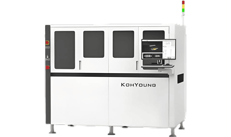
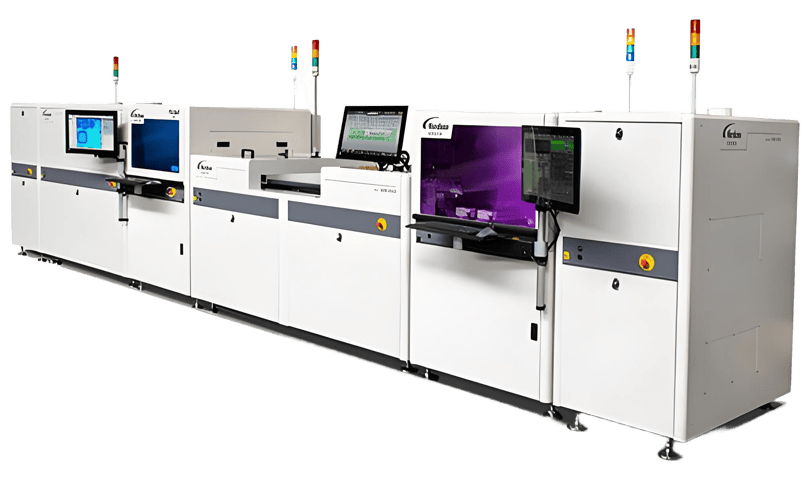
With the growing demand for electronics, products are increasingly miniaturized. This trend presents challenges in managing the contact area and spacing between miniature components and substrates (such as 0201 chips, and high-density, fine-pitch BGA and CSP array components).
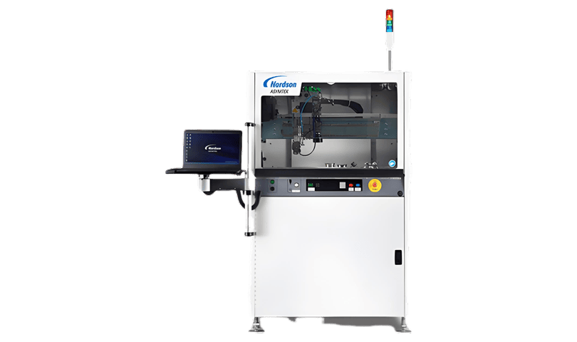
To address this, Jeenoce introduced SPI equipment from a leading Korean manufacturer with 16 years of expertise in solder paste inspection.
Through comprehensive solder paste printing quality management—encompassing hardware configuration and software algorithm upgrades—this system helps customers minimize losses in the initial stage of the SMT assembly process—solder paste printing.
With the growing demand for electronics, products are increasingly miniaturized. This trend presents challenges in managing the contact area and spacing between miniature components and substrates (such as 0201 chips, and high-density, fine-pitch BGA and CSP array components).
To address this, Jeenoce introduced SPI equipment from a leading Korean manufacturer with 16 years of expertise in solder paste inspection.
Through comprehensive solder paste printing quality management—encompassing hardware configuration and software algorithm upgrades—this system helps customers minimize losses in the initial stage of the SMT assembly process—solder paste printing.
Why is solder paste inspection so important for the whole SMT assembly process?
Many electronics manufacturing practitioners might assume that post-reflow X-Ray or AOI inspection is the most critical factor for yield. However, global SMT industry statistics indicate that solder paste printing alone accounts for nearly 80% of yield impact.
This means that implementing inspection right after solder paste printing can prevent up to 80% of potential defects, compared to only finding them after reflow soldering.
It not only indirectly saves rework costs for manufacturers but also delivers additional benefits. The associated cost is merely adding one inspection step—a step becoming increasingly crucial given the ongoing trend towards component miniaturization and refinement.
For example, the adoption of 01005 passive components, ultra-fine pitch QFP technology, and lead-free solder paste can significantly increase the process defect rate.
What problems can solder paste inspection equipment solve?
The equipment's name clearly indicates its purpose——detecting solder paste defects. Therefore, the key question is—what types of defects occur during the solder paste printing process?
Solder Paste Printing (SPI) Defects |
Abnormal Solder Paste Volume | Insufficient solder paste (leading to weak joints/poor connections), excessive solder paste (causing component short circuits) |
Printing accuracy issues | Misalignment (failure to align with pads), offset (printing position deviates from design) |
Shape abnormalities | Collapse (excessive spreading) |
Solder ball abnormalities | Excess solder balls around pads |
Blurred printing | Smudged or disorganized solder paste application |
Shape abnormalities | Irregular solder paste printing or blurred edges |
Assembly Process Defects |
Component Installation Issues | Component offset, missing or extra components, polarity errors, skew, inversion, installation failures, poor adhesive alignment, etc |
Solder Joint Quality Issues | Excessive solder, height defects, insufficient solder around pins, under-soldered joints, pin lifting, bridging errors, volume defects, tombstoning, etc |
Furthermore, the solder paste inspection (SPI) system introduced by Jeenoce not only detects solder paste printing defects but also identifies dust and metal debris on the PCB that could impair performance or cause short circuits.
Additional capabilities include conductive adhesive inspection and detection of electrode preparation issues. All findings are presented visually in full-color images.
What is the working principle of the solder paste inspection system introduced by Jeenoce?
Jeenoce's partner, a Korean manufacturer, is a long-standing expert in solder paste and optical inspection, having continually advanced solder paste detection technology for decades.
The system primarily utilizes a combination of laser triangulation, phase-shifting profilometry, optical imaging with vision algorithms, and a data-integrated AI system. This synergy enables SMT assembly factories to identify issues promptly and prevent significant losses.
Laser Triangulation Technology
Laser triangulation technology works by projecting a laser onto the solder paste surface. A camera captures the reflection, and algorithms use this data to calculate the height, area, and volume of the solder paste deposits.
Phase-Modulated Profile Measurement Technology
This technique projects specific light patterns (fringes) onto the target surface. Deformations in these patterns, captured from multiple angles, are used to calculate height and contour information.
Optical Imaging Technology Combined with Vision Algorithms
The optical imaging system captures images of the printed circuit board. These images are analyzed by vision algorithms using a "virtual reference" or golden board comparison method. This involves comparing the captured images against an ideal reference to evaluate solder paste presence, alignment, and shape based on pre-defined criteria.
Data integration AI system
Data from these technologies is integrated into a systematic database within the software. To ensure high accuracy, specialized algorithms compensate for potential PCB warping, including bow, twist, and other distortions.
Ultimately, the process control system, leveraging proprietary 3D measurement patents and AI algorithms, provides clear, intuitive, and highly reliable results.
It's worth explaining why only we call it solder paste detection system?
The system features unique self-diagnostic and automatic rework functions. Predictive maintenance plans help prevent unexpected downtime. Automated solution guidance helps prevent costly errors.
The fundamental differences between 2D and 3D solder paste inspection technologies
Inspection scenari | 2D | 3D |
Large pads (e,g,, BGA) | Can be used but is not accurate | High accuracy |
Small pads (e,g,, 0201) | Error > 15% | Error < 5% |
Height anomalies (voids, offset issues) | May miss defect | Direct measurement |
Advanced SPI systems often integrate both 2D and 3D inspection capabilities.
3D measurement is crucial innovation, as miniaturized PCB components require volumetric and height data that simple 2D inspection cannot provide for detecting certain defects.
What is the workflow of the solder paste inspection system introduced by Jeenoce?
")
Why choose the SPI solder paste inspection system in Jeenoce’s SMT whole line solution system?
Suitable for high speed production line testing speed
Fully match the rhythm of the production line to easily undertake high-speed testing requirements.
By expanding the field of view, the throughput per unit time of detection is increased to improve the efficiency of the link.
Adapt to different sizes of PCB products to be tested to solve the problem of identification difficulties.

Industry's first precision presentation
Patented "Warping Compensation" technology counteracts PCB deformation or unevenness.
Highly advanced 3D scanning technology combined with AI-driven analysis capabilities increases accuracy.
Shadowless Mohr technology solves shadow and scattering problems and eliminates irregular shadow interference.
"Perfect digital PCB template" compared with actual production PCB to overcome nonlinear problems.

Guarantee mechanism for the whole production cycle
Real-time SPC monitoring mechanism helps optimize production efficiency from overall production process trend analysis.
The closed-loop feedback system automatically adjusts stencil printer parameters and feeds data back to optimize the printing process.
Archived inspection data can be integrated with MES systems for traceability and detailed process analysis.
Increases efficiency by reducing board scrap and rework, delivering direct cost savings and ROI.

Solutions for ultra-long products
Handles ultra-long boards (1300-1800mm) used in specialized fields like electric vehicles, communications, and data storage. (Contact our engineering team for specific requirements).
Supports one-pass inspection of ultra-long circuit boards, simplifying the testing process.
Offers fully automatic, inline solutions requiring no manual intervention, seamlessly integrating into factory production rhythms.

Meets the highest standards of customers and industry
Jeenoce acts as a solution integrator, providing tailored, one-stop intelligent upgrade solutions for your SMT line.
Provides comprehensive end-to-end support, including pre-sales consultation, solution design, testing, delivery, and post-sales service.