Advanced packaging semiconductor void-free contact welding (joining) process
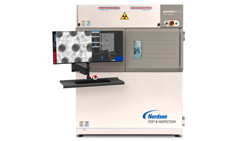
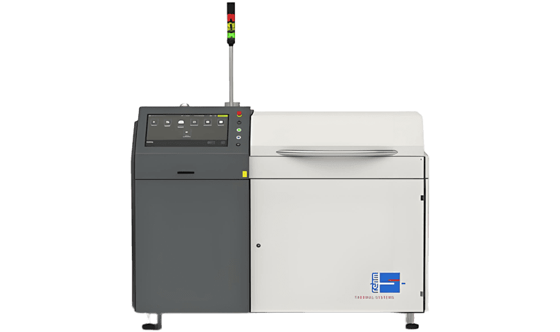
Contact welding(welding) is a kind of welding method for DCB to process substrate mainly (most) semiconductor products in vacuum environment through "teppan firing" process,Jeenoce is positioned as the middle and high-end SMT equipment solution integrator to introduce this equipment mainly to help semiconductor manufacturing customers to accelerate the production pace while producing high yield semiconductor products with the lowest void rate.
It should be noted that the difference between contact welding and pressure welding, formic acid reflow welding,the contact welding equipment adopted by Jeenoce is a special surface heating welding process (or thermal radiation and heat conduction) for the semiconductor industry, rather than pressure welding by mechanical pressing.
Although formic acid can be used to reduce the void rate and remove the surface oxidation problem caused by the welding process,but their processing technology is slightly different because of the different product types.