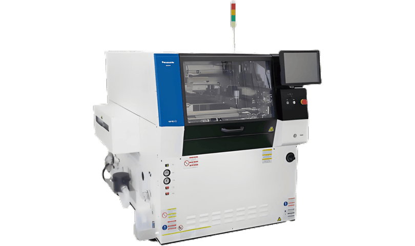
X-ray inspection for PCB is a powerful technology that lets you see inside printed circuit boards without taking them apart. It uses high-resolution X-ray imaging to detect hidden defects like solder joint issues, voids, and misalignments that traditional optical inspection can miss. This makes it essential for maintaining quality in complex electronics manufacturing.
At Jeenoce, we integrate smart manufacturing solutions with advanced X-ray PCB inspection systems, providing seamless automation for your SMT lines. Our equipment supports real-time quality control, helping you catch problems early, reduce waste, and improve yield. This technology is ideal for industries requiring precise inspection — from consumer electronics and automotive modules to aerospace and medical devices.
For more details on how our X-ray systems support electronics manufacturing, check out our in-depth industry solutions. And to understand the technical side better, our technical insights offer a detailed look at the inspection technology and automation benefits.
Our X-ray PCB inspection system combines advanced imaging technology with a robust defect detection suite to ensure your boards meet the highest standards. Here’s what makes it stand out:
Advanced Imaging Technology
Microfocus X-ray source for clear, high-resolution images
3D X-ray tomography available on select models for multilayer PCB inspection
Real-time imaging for faster decision-making on the production line
Comprehensive Defect Detection
Detects solder joint voids, solder bridges, and micro cracks
Identifies hidden defects including BGA solder joint analysis and PCB void detection imaging
Automated reporting to flag issues immediately
Flexible Operational Modes
| Mode | Use Case | Benefit |
|---|---|---|
| Inline Inspection | Real-time screening during SMT | Continuous quality control |
| Offline Analysis | Detailed defect investigation | In-depth root cause analysis |
| Batch Mode | Multiple PCBs scanned sequentially | Efficient throughput for volume |
Seamless Software Integration
Compatible with major SMT line management software
User-friendly interface with customizable inspection parameters
Data export options for SPC and production analytics
Safety and Compliance
Fully shielded chamber meeting FDA radiation safety standards
Automatic safety interlocks and alerts
Designed to comply with international safety regulations
Explore our full range of capabilities and how they fit into smart manufacturing environments, such as those detailed in Jeenoce’s smart production solutions, to boost your line’s efficiency and reliability. More details on Jeenoce’s manufacturing integration are available.
The X-ray process works by accelerating electrons with high voltage and directing them to hit a metal target. This generates powerful, penetrating X-rays.
When these rays interact with the atoms in a circuit board, some are absorbed, and others pass through.
The transmitted rays are captured by a detector, and then analyzed by computer software to identify internal structures or defects.
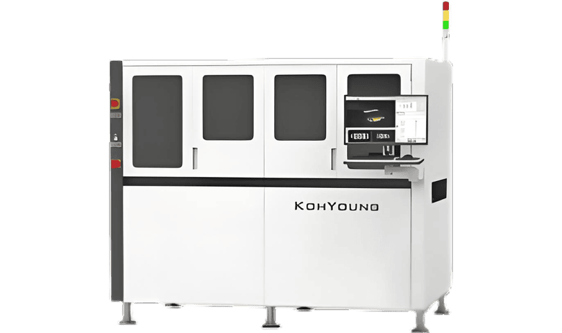
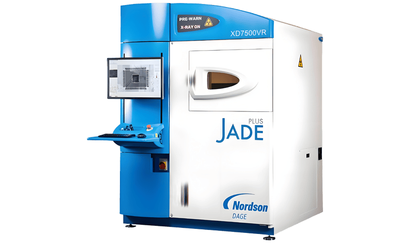
The Brand Behind Jeenoce’PCB X-ray Inspection Equipment
The X-ray inspection machine comes from a UK-based company that has specialized in PCB, semiconductor, and other high-end inspection fields for decades. It's a leader in non-destructive testing with strong industry recognition.
PCB inspection equipment includes:
AOI (Automated Optical Inspection) based on optical principles, including 3D AOI.
X-ray inspection systems, both 2D and 3D.
Other functional test equipment.
Optical and X-ray inspections often work in tandem, complementing each other.
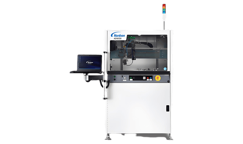
Our X-ray PCB inspection system is built with precision and versatility to meet your production needs. Below is a detailed overview of the core specifications, with advanced features expandable for deeper insights.
Imaging Specs
Resolution | <0.95 μm |
Max Voltage | 160 kV |
Target Power | 3W |
Magnification | 2000–7000× (at various angles) |
Max Inspection Area | 508 × 445 mm (customizable) |
CMOS Detector Resolution | 1.33 Megapixels |
Imaging Software | UK Patent |
Radiation Leakage | <1μSv/hr |
OS | Windows 10 (64-bit) |
Machine Specs
Size | 1450 × 1700 × 1970 mm |
Weight | 1950 kg |
Max Sample Weight | 5 kg |
Power Supply | 200–230V, 16A (Single-phase) |
Max Power | 1000W |
Advanced Specifications
Advanced Feature Details 3D Tomography Resolution Up to 5 µm Automated Defect Recognition AI-powered analysis engine Data Export Formats CSV, XML, proprietary JEENOCE formats Integration Options Inline SMT conveyor system ready Remote Access Secure network-based control and monitoring Maintenance Predictive diagnostics with alert system
This level of detail ensures you get thorough quality control without slowing your production line. For specifics on deployment and custom setups, check out our smart manufacturing integration solutions.
X-ray for PCB inspection plays a vital role in modern SMT and electronics manufacturing. It excels in BGA and fine-pitch inspection, where traditional optical methods often fall short. The ability to see beneath the surface helps detect hidden solder joint issues like voids and bridges, ensuring reliable solder connections in complex assemblies.
For multilayer PCB analysis, microfocus X-ray technology reveals internal layers and buried defects without damaging the board. This non-destructive method is essential for verifying layer alignment, detecting delamination, and identifying internal cracks — critical for high-density and multilayer boards.
In component verification, the system inspects small and densely packed parts like ball grid arrays, chips, and connectors to confirm placement accuracy and solder quality. It supports real-time quality control on assembly lines, minimizing rework and production delays.
Inspection Targets & Typical Defects
Component / Application | Key Detectable Defects |
SMD, BGA | Missing balls, cold joints, short circuits, ball misalignment, excessive voiding (esp. multilayer joints) |
CSP / Flip Chip | Poor ball wetting, alignment errors at micron scale |
QFP / LGA | Lifted pins, insufficient solder, bridging (especially in dense packages) |
SMT solder joints | Inconsistencies between pads and leads/balls: poor wetting, cold joints, solder splash |
Multilayer board vias | Integrity of plated through, blind, or buried vias (cracks, voids) |
FPC / Rigid-Flex PCBs | Fatigue cracks in bend areas, delamination |
PCBA Modules | Solder defects under components like shields or heatsinks |
Modular Devices | Internal weld quality of power, RF, MEMS sensor modules |
Semiconductor Substrates | Solder joints between chips and substrates |
Automotive Electronics | ECU internal joints, wire harness connections, component stability |
Precision Castings | Porosity, fatigue cracks in aluminum die-casting, internal gear defects |
New Energy/Batteries | Battery cell alignment, tab welds, foreign object detection |
Solar Components | Cracked welds on wafers, solder uniformity, connector corrosion |
Industry spotlights include aerospace, automotive electronics, medical devices, and consumer electronics, where device reliability is paramount and failure costs are high. Integrating our advanced X-ray inspection ensures your production meets strict quality standards while boosting efficiency.
Explore how Jeenoce’s X-ray inspection technology fits seamlessly into your SMT line with flexible options tailored for different production scales and complexities.
Investing in an X-ray PCB inspection system delivers real, measurable benefits for your assembly line. Here’s what you can expect:
Quality Assurance Gains
Catch defects early: Identify solder voids, bridges, and misalignments before they cause failures.
Improve product reliability: Reduce field returns and warranty claims with thorough inspection.
Consistent quality: Automated X-ray inspection ensures every PCB meets your standards—no exceptions.
Efficiency Boost
Faster inspections: Real-time X-ray electronics quality control speeds up your testing process.
Lower rework rates: Detect issues immediately to avoid costly manual repairs later.
Seamless integration: Inline SMT X-ray machines fit right into existing manufacturing lines for minimal disruption.
Cost Savings
Reduce scrap: Spot hidden defects like PCB void detection imaging, cutting waste.
Lower labor costs: Automation reduces the need for manual inspection and interpretation.
Minimize downtime: Early detection speeds troubleshooting and keeps production running smoothly.
Real-World Impact
| Benefit | Typical ROI Effect |
|---|---|
| Defect reduction | Up to 30% fewer defects |
| Inspection speed | 2x faster throughput |
| Cost savings | 20-40% lower scrap costs |
| Warranty claims | Decreased up to 50% |
One of our Thai customers in electronics manufacturing reported a 25% boost in yield within the first three months of implementing our automated X-ray inspection system.You can explore more success stories and insights in our latest news on smart manufacturing.
Maximize your production line’s performance and bottom line with advanced X-ray PCB inspection tech from Jeenoce.
Explore our interactive X-ray samples gallery to see real-world examples of PCB defect detection. From solder joint voids to solder bridge identification, these high-resolution X-ray pictures of PCB inspection machines highlight common issues like bubbles and hidden faults without damaging your boards.
Watch our detailed video demo showcasing Jeenoce’s X-ray inspection systems in action—perfect for spotting defects in multilayer boards and BGA solder joints. Plus, get user tips on how to interpret images and optimize inspection settings for your SMT line.
These resources help you understand how advanced X-ray PCB solder joint inspection can catch issues early, ensuring your production maintains the highest quality standards.
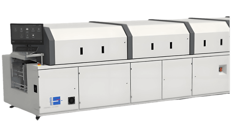
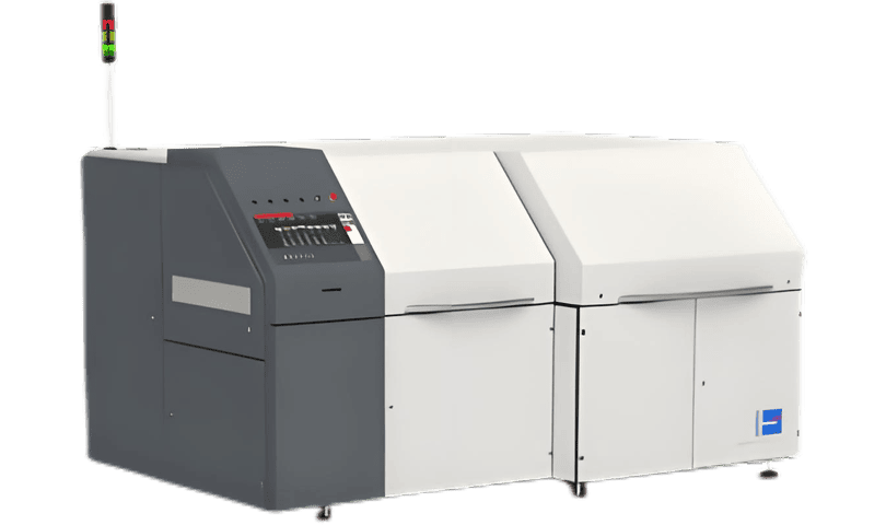
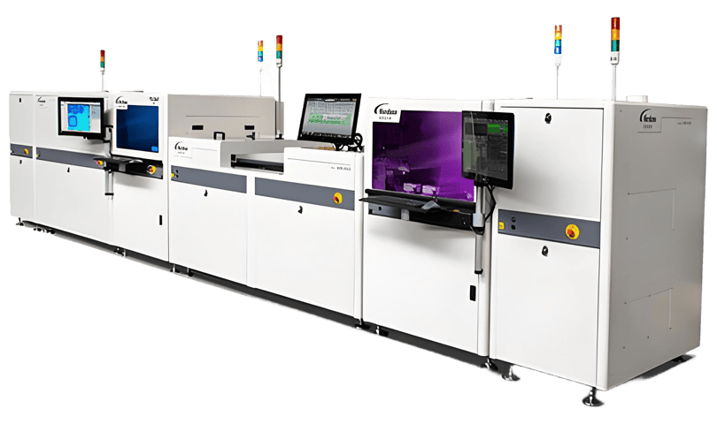
Our X-ray PCB inspection systems are designed to fit seamlessly into your existing SMT production lines. Whether you’re running a small batch or a high-volume operation, we offer flexible integration to keep your workflow smooth and efficient.
SMT Line Compatibility
Supports major SMT equipment brands
Inline-ready for real-time quality control
Easily connects with automated pick-and-place and reflow ovens
Customization Tiers
| Tier | Features | Ideal For |
|---|---|---|
| Standard | Default imaging modes, basic defect detection | Small to mid-sized production lines |
| Advanced | 3D tomography, AI-based solder joint analysis | Multilayer PCBs, high complexity |
| Premium | Fully tailored software & hardware integration | Large-scale plants, custom workflows |
Easy Setup Guide
Plug-and-play hardware with step-by-step instructions
Infographic walkthrough for rapid deployment
Remote support available during installation
For manufacturers focused on efficient integration and continuous improvement, Jeenoce’s smart manufacturing expertise ensures that setup and customization are hassle-free. Discover more about our approach on the smart manufacturing integration page.
With this flexible system, you can tailor your X-ray inspection solution to match your production needs without overspending or compromising on quality.
Finding the right X-ray for PCB inspection that fits your budget and needs is simple with our clear pricing tiers and easy model selection. Whether you’re upgrading a single SMT line or setting up a full-scale smart manufacturing system, we offer flexible options designed to deliver value and performance.
Pricing Tiers: Choose from entry-level models for straightforward PCB solder joint inspection up to advanced systems featuring 3D X-ray tomography and real-time defect detection.
Model Selector Tool: Use our intuitive online tool to compare features, specs, and prices, helping you pick the perfect fit for your production workload.
Request a Quote: Ready to make the move? Contact us for a custom quote tailored to your manufacturing setup.
Authorized Distributors: We partner with reliable distributors across the globe to ensure fast delivery, professional installation, and ongoing support.
Explore our detailed models and pricing options to get the most out of your inline SMT X-ray machine investment. For a closer look at our solutions in action, check our successful customer case studies or explore the smart manufacturing integration on the semi-automated inspection page.
Q1: What is X-ray inspection for PCB?
X-ray inspection for PCB is a non-destructive testing method that uses X-rays to see inside printed circuit boards. It helps detect hidden defects like solder joint issues, voids, and misaligned components without damaging the board.
Q2: How does Jeenoce’s X-ray system integrate with SMT lines?
Jeenoce’s inline SMT X-ray machine fits seamlessly into automated production lines, offering real-time quality control and defect detection. It supports advanced imaging and connects with factory software for smooth data management and reporting.
Q3: Can this system detect BGA solder joint defects?
Yes. Our system specializes in BGA solder joint analysis and uses microfocus X-ray technology to inspect fine-pitch components and multilayer boards, identifying solder bridges, voids, and other critical defects.
Q4: Is the X-ray inspection safe for electronics and operators?
Absolutely. The system is built with robust safety features and complies with all relevant U.S. radiation regulations, ensuring safe operation around sensitive electronics and personnel.
Q5: What types of PCBs can this X-ray system inspect?
We support a wide range—from single-layer to complex multilayer PCBs, including those with high-density ball grid arrays (BGAs) and other advanced electronics components.
Q6: How do I choose the right model and features for my line?
Jeenoce offers customizable tiers and models tailored to different production needs and budgets. Contact our team for personalized recommendations and quotes.
Our customers in the Southeast Asian electronics manufacturing sector consistently praise our X-ray PCB inspection systems for their accuracy and reliability. Here’s what a few verified users have to say:
“Since integrating Jeenoce’s automated X-ray inspection system, our defect detection rate has improved by 30%. The ease of use and real-time quality control save us valuable production time.” – Production Manager, Electronics Manufacturer in Thailand
“The microfocus X-ray technology gave us clear insight into BGA solder joint issues we couldn’t see before. This tool has become essential for our SMT line.” – Quality Control Engineer, PCB Assembler in Malaysia
“Jeenoce’s customization options allowed us to tailor the inspection system to our multilayer PCB needs, raising our throughput without sacrificing accuracy.” – Operations Lead, Electronics Firm in Vietnam
To support you beyond purchase, we offer a robust resource hub packed with detailed manuals, video demos, and tips for optimizing inspection workflows. Our resources are designed to help East Asian and Southeast Asian manufacturers get the most from our non-destructive PCB defect scanners. For deeper insights into our technology and integration support, visit our Smart Manufacturing Solutions page.
Trust signals like ISO certifications and compliance with U.S. safety standards back our commitment to quality and reliability. Coupled with our customer-first approach and proven performance in real-world applications, Jeenoce stands out as a dependable partner for your X-ray PCB solder joint inspection needs.
Even the tiniest flaws have nowhere to hide
2000–7000× magnification from any angle to spot any defect
Real-time, high-definition display under tough conditions
Up to 160kV, perfect for high-density PCBs

Automatically or manually select target components for defect analysis
Detect and measure chip-level bubbles and void ratios
Click directly on the screen to zoom in/out on suspect areas
Minimal training required — intuitive interface anyone can use

Dual-layer glass prevents radiation leaks
Built-in smart interlocks: no operation if the door isn’t fully closed
Meets or exceeds radiation leakage limits in all countries

Open-tube design — just replace the filament for long-term use(If you have semiconductor inspection needs, our X-ray inspection equipment tailored for semiconductors is the ideal choice.)
Engineered for long hours of operation without damage
Outperforms many competitors in durability and lifespan
Continuously upgraded by an industry-leading supplier
Compliant parts and proper maintenance = years of worry-free use


Message