Scanning Acoustic Microscopy (SAM) is an ultrasound-based non-destructive testing (NDT) technique used to visualize and analyze internal structures of materials. It works by transmitting high-frequency sound waves into a sample, then detecting how these waves reflect or pass through different layers based on acoustic impedance contrasts. This allows us to detect flaws such as voids, delamination, and cracks without damaging the item under inspection.
How SAM Works
The core of SAM is a precision transducer that scans the sample’s surface, sending pulses and capturing reflected signals. These reflections vary depending on material density and interfaces inside the sample.
A-Scan: Shows signal amplitude versus time, revealing depth information at a single point.
B-Scan: Produces a cross-sectional image by stacking A-Scans along a line.
C-Mode: Offers a two-dimensional top-down map of internal features across the scanned area.
Bulk-Scan:By obtaining internal images of the product, we assess its uniformity and continuity to determine whether the product has defects.
PolyGate™ & Multi-Scan:A mode that simultaneously excites and scans multiple layers, thereby collecting signals from these layers to generate images.
Q-BAM™:Intuitively observes a sample’s internal structure and enables in-depth analysis via polarity/amplitude data, suitable for scenarios requiring both visualization and quantitative testing (e.g., precision manufacturing, biomedicine, material R&D).
Surface-Scan:A mode that scans a product’s surface and subsurface to detect defects.
AutoScan™:Fully automatic scanning mode: programmed according to requirements to obtain all required scanning data in one go.
THRU-Scan™:Via "penetrating ultrasonic projection," it delivers a macroscopic full-thickness defect overview of the sample, suitable for scenarios needing quick identification of through-through issues (e.g., industrial preliminary screening, large-scale quality inspection).
3V™:Construct 3D stereoscopic images from existing ultrasonic images.
3D TOF:"3D TOF" (3D Time of Flight) is an imaging technology based on ultrasonic propagation time. Core value: converting "time" to "space" — via precise ultrasonic flight time calculation, it builds a 3D "digital twin" of the object’s interior, ideal for scenarios needing quantification of defects’ spatial locations (high-precision inspection: aerospace, semiconductors, etc.).
Multi-Axis Scan™:Scanning imaging mode for spherical or curved surface products.
R-Scan™:For cylindrical products: via rotation to achieve full cylindrical inspection.
STaR™:STaR™ simultaneously verifies packaging integrity (transmission) and internal connection quality (reflection), ensuring global production line consistency via unified image standards — typically for inspecting transport-related defects.
Visualizing these acoustic wave interactions highlights defects invisible to optical or standard imaging.
Jeenoce’s Unique Advantage
Jeenoce’s SAM systems stand out by seamlessly integrating directly into Surface Mount Technology (SMT) production lines. This inline quality control enables real-time defect detection during manufacturing, minimizing yield loss and boosting throughput—ideal for smart factories looking for efficiency without pausing production.
Our Scanning Acoustic Microscopy (SAM) system offers flexible, powerful features designed for precise defect detection and smooth integration in manufacturing lines.
Flexible Transducer Frequencies
Frequency range: 5 MHz to 400 MHz
Benefit: Choose low frequencies for deeper penetration or high frequencies for detailed resolution
Immersion and Tankless Options
Supports both immersion setups (ideal for small, delicate samples) and tankless scanning for larger or fragile parts
Adaptable to a wide variety of sample sizes and shapes
Advanced Software Suite
Real-time 3D imaging: Visualize internal structures instantly
AI-assisted defect classification: Speeds up identifying voids, delamination, or cracks
ERP data export: Seamlessly share inspection results with manufacturing management systems
Automation and Integration
Comes with an API that allows robotic handling and automation in non-standard or complex setups
Perfect for inline Acoustic Micro Imaging on SMT lines and automated production environments
| Feature | Details |
|---|---|
| Transducer Frequencies | 5–400MHz |
| Imaging Modes | Real-time 3D, A-Scan, B-Scan, C-Scan,Bulk-Scan,PolyGate™ & Multi-Scan,Q-BAM™,Surface-Scan,AutoScan™,THRU-Scan™,3V™,3D TOF,Multi-Axis Scan™,R-Scan™,STaR™ |
| Sample Handling | Immersion & Tankless options |
| Software Capabilities | AI defect classification, ERP export |
| Automation Support | API for robot integration |
These features make our SAM solution adaptable, efficient, and ideal for high-throughput environments needing reliable, ultrasonic non-destructive testing.
Here’s a quick overview of the key specs for our SAM system, designed to fit varied industrial needs:
| Feature | Details |
|---|---|
| Frequency Range | 5MHz–400MHz |
| Resolution | Down to 10μm (depends on frequency) |
| Max Sample Size | 0.5 to 350mm |
| Imaging Modes | Real-time 3D, A-Scan, B-Scan, C-Scan,Bulk-Scan,PolyGate™ & Multi-Scan,Q-BAM™,Surface-Scan,AutoScan™,THRU-Scan™,3V™,3D TOF,Multi-Axis Scan™,R-Scan™,STaR™ |
Interfaces
USB 3.0 for fast data transfer
Ethernet for network integration
Custom API for automation and robotics
Compliance & Standards
ISO 9001 Certified
CE Marked for safety and quality standards
This combination of specs lets you handle everything from tiny semiconductor wafers to larger PCB panels swiftly, with reliable image quality and compatibility for factory automation.
Scanning Acoustic Microscopy (SAM) plays a vital role in smart manufacturing by spotting hidden defects early on, saving time and cost. Here’s where it shines:
Delamination detection in PCBs: SAM identifies layers separating beneath the surface, which is critical before assembly.
Void detection in die bonds: Small air pockets inside die attachments can cause failures; SAM spots these reliably.
Crack analysis in power modules: It finds micro-cracks in power electronics that could lead to breakdowns.
Wafer-level inspections: SAM inspects thin wafers for defects without damage, supporting semiconductor quality control.
A recent case study showed a 25% reduction in yield loss on SMT lines after integrating inline SAM inspections. This means fewer defects pass through, boosting overall production efficiency and lowering rework costs.
In short, SAM helps keep your manufacturing smart, efficient, and defect-free.
Using Scanning Acoustic Microscopy (SAM) pays off quickly by spotting defects early and saving on costly reworks. It’s perfect for boosting throughput in automated SMT lines, keeping production smooth and efficient.
Key Benefits:
Early Defect Detection: Find hidden issues like voids or delamination before they cause failures.
Lower Rework Costs: Catch faults early, avoid expensive scrap or repairs later.
Faster Production: Inline SAM integration speeds up inspection without slowing down your workflow.
Improved Yield: Higher quality checks lead to fewer defects slipping through, increasing overall output.
ROI Snapshot – Before vs After SAM Implementation
| Metric | Before SAM | After SAM | Improvement |
|---|---|---|---|
| Defect Rate | 8% | 2% | 75% Reduction |
| Rework Costs | High | Significantly Lower | Up to 40% Savings |
| Inspection Speed | Manual & Slow | Automated & Fast | 3x Faster |
| Overall Yield | Moderate | High | 25% Increase |
Integrating SAM into your production line means fewer surprises, less downtime, and better control over quality. It’s a smart investment that pays off in saved time, money, and improved product reliability.
Jeenoce offers a range of products and accessories that enhance your Scanning Acoustic Microscopy (SAM) experience and ensure seamless integration with your SMT lines.
Key Products
Jeenoce SMT Integration Kits
Designed for easy inline inspection, these kits enable real-time quality control without slowing your production.
Custom Transducers
Choose from a wide frequency range (5-400 MHz) to match your resolution and penetration needs.
Analysis Software Upgrades
Boost defect detection accuracy with AI-assisted classification, real-time 3D imaging, and direct ERP data export.
Comparison Chart: Jeenoce SAM vs Traditional Methods
| Feature | Jeenoce SAM | X-ray Inspection | Optical Microscopy |
|---|---|---|---|
| Non-destructive | ✔ | ✔ | ✔ |
| Detection of Voids | Excellent (C-SAM, Through-Transmission) | Limited | Poor |
| Resolution Range | Up to 400 MHz frequency | Moderate | High (surface only) |
| Throughput | Fast | Slower | Faster but surface-only |
| Inline SMT Integration | Seamless with API | Difficult | Not feasible |
| Radiation-Free | ✔ (Ultrasound-based) | ✘ (Ionizing radiation) | ✔ |
| Setup & Sample Prep | Minimal | Moderate | Minimal |
Jeenoce’s SAM products and accessories bring advanced acoustic microscopic inspection to your smart manufacturing setup — giving you faster, safer, and more detailed analyses than traditional X-ray or optical options.
“We integrated Jeenoce’s Scanning Acoustic Microscopy into our SMT line, and the impact was immediate—defect detection improved, and yield rates went up by over 20%. The inline system fits perfectly with our existing setup.” – Electronics Manufacturing Manager, Thailand
“Jeenoce’s SAM technology helped us catch hidden voids and delamination early, saving both time and money on rework. The software is intuitive, and the support team is always responsive.” – Quality Control Lead, India
We’re here to make sure you get the most from your Scanning Acoustic Microscopy system with flexible support options tailored to your needs:
Installation: Expert technicians handle setup to get you up and running quickly.
Training: Hands-on sessions to help your team master SAM operation and analysis.
24/7 Remote Diagnostics: Fast troubleshooting and support whenever you need it, minimizing downtime.
Have questions or ready to buy? Click Get a Quote to receive personalized information.
Contact Information:
Reach out anytime via phone, email, or our online chat.
Certified to ISO 9001 standards and CE marked, ensuring top-quality and compliance you can trust.
Scanning Acoustic Microscopy (SAM) works by sending high-frequency sound waves through a sample to reveal its internal structure. The core idea is acoustic wave propagation—sound waves travel through materials and change depending on what they hit. When these waves encounter differences in material density or elasticity, known as acoustic impedance contrasts, some waves reflect back while others pass through. This reflection and transmission pattern helps us map hidden features like voids, cracks, or delamination.
Key concepts that make this possible include:
Acoustic impedance matching: Ensures the sound waves move efficiently between the transducer, coupling medium (usually water or gel), and the sample.
Reflection and transmission: Variations in impedance cause waves to bounce back or continue, which the system then detects.
SAM uses different scanning modes to visualize the data:
A-Scan: A single-point measurement of reflected wave amplitude over time—think of it as a depth profile.
B-Scan: Cross-sectional images created by moving the transducer across the sample, showing depth and internal layers.
C-Mode: A top-down view, showing a 2D map of features at a specific depth.
Bulk-Scan: Obtains internal product images to assess uniformity and continuity — used to determine product defects.PolyGate™ & Multi-Scan: Simultaneously excites and scans multiple layers, collecting signals to generate images — a multi-layer imaging mode.Q-BAM™: Intuitively observes a sample’s internal structure and enables in-depth analysis via polarity/amplitude data — suitable for scenarios requiring both visualization and quantitative testing.Surface-Scan: Scans a product’s surface and subsurface to detect defects — a mode for surface and shallow defect inspection.AutoScan™: Fully automatic scanning programmed to requirements, acquiring all needed data in one go — an efficient batch data collection mode.THRU-Scan™: Delivers a macroscopic full-thickness defect overview via penetrating ultrasonic projection — ideal for quick preliminary screening of through-through issues.3V™: Constructs 3D stereoscopic images from existing ultrasonic images — an ultrasonic data 3D visualization mode.3D TOF: An imaging technology based on ultrasonic propagation time, converting "time" to "space" to build a 3D internal digital twin — a high-precision solution for quantifying defects’ spatial locations.Multi-Axis Scan™: Scanning imaging for spherical or curved surface products — a dedicated mode for irregularly shaped structures.R-Scan™: Achieves full cylindrical inspection via rotation for cylindrical products — a comprehensive inspection solution for cylindrical items.STaR™: Simultaneously verifies packaging integrity (transmission) and internal connection quality (reflection), ensuring global production line consistency via unified image standards — typically for inspecting transport-related defects.
Historically, acoustic microscopy evolved from classic ultrasound techniques, gaining higher frequencies (up to several hundred MHz) for finer resolution. This advancement made embedded wave interaction diagrams possible, illustrating how waves bounce inside complex materials.
By understanding these principles and scanning modes, we can harness SAM to inspect electronics, materials, and assemblies non-destructively with high precision.
Jeenoce’s Scanning Acoustic Microscopy system is built around smart, flexible tech designed to fit various inspection needs in smart manufacturing. Here’s what makes it stand out:
Advanced Transducer Technology:
Offers a wide range of frequencies—from 5MHz up to 400MHz. This balance lets you choose higher frequencies for fine detail (resolution) or lower ones for deeper penetration, depending on your sample type.
Powerful Imaging Software:
Includes automated void quantification that speeds up defect detection, plus 3D reconstruction to give a clear, real-time view of internal structures. AI-assisted features help classify defects quickly and accurately.
Scalable Hardware Design:
Built to grow with your process—from R&D labs to full production lines. Compact and modular, it fits seamlessly whether you’re running small batches or hundreds of units daily.
Seamless PLC Integration for SMT Lines:
Connects smoothly with your existing programmable logic controllers (PLCs), making inline inspection part of your smart manufacturing workflow. This means real-time quality control without slowing down your SMT line.
Together, these components make Jeenoce’s SAM system a reliable, scalable solution for detecting hidden defects like voids or delamination early, saving time and cost in electronics manufacturing.
Scanning Acoustic Microscopy (SAM) plays a critical role in inspecting semiconductors and PCBs, especially for detecting die-attach voids and delamination. These issues can cause device failures, so early detection is key to maintaining high quality.
In power electronics, SAM helps identify gas pockets and cracks that affect performance and reliability. This ensures components operate safely under high stress.
Hybrid assemblies, which combine different materials and technologies, often require custom SAM scans. This flexibility allows detailed internal imaging tailored to complex designs.
Real-world results back SAM’s effectiveness: industry case studies report a 20-30% reduction in defects after integrating SAM inspection into production lines. This leads to lower scrap rates and better product yield.
By using SAM for non-destructive failure analysis and acoustic micro imaging, manufacturers can improve quality control, reduce rework, and keep ramps running smoothly.
Jeenoce Scanning Acoustic Microscopy (SAM) stands out compared to X-ray and CT scanning, especially for smart manufacturing and SMT line integration. Here’s how it compares:
| Feature | Jeenoce SAM | X-ray / CT Scanning |
|---|---|---|
| Cost | Lower operational cost | Higher equipment & safety cost |
| Speed | Up to 500 mm²/s scanning | Slower, longer scan times |
| Sample Prep | Minimal, no special prep | Often complex sample setup |
| Safety | Eco-friendly, no radiation | Uses ionizing radiation |
| Resolution | High-frequency ultrasound | Good for dense materials |
| Non-Destructive | 100% non-destructive | Non-destructive but limited by radiation |
| Automation | Seamless inline SMT integration | Limited inline capabilities |
| Predictive Maintenance | Acoustic imaging detects early defects | Limited early detection |
Why Choose Jeenoce SAM?
Fast inspections speed up quality checks without slowing production.
No radiation risk means safer use on the factory floor.
Easy integration with robotic and PLC systems for automated lines.
Detects hidden defects like delamination and voids early, reducing costly rework.
Environmentally friendly, no hazardous waste or special disposal needed.
Jeenoce SAM’s practical benefits fit well in smart factories aiming for reliable, fast, and eco-safe non-destructive testing.
Picking the right Scanning Acoustic Microscopy (SAM) system depends on what you’re inspecting, how fast you need results, and your budget. Here’s a simple guide to help you make the best choice, focusing on Jeenoce’s SAM lineup designed for global smart manufacturing needs.
Buyer Guide: Key Factors to Consider
| Factor | What to Think About |
|---|---|
| Sample Types | Are you scanning PCBs, wafers, power modules, or hybrid electronics? Each needs different resolution and size accommodations. |
| Throughput | How many parts per hour? Inline SMT lines push for rapid scans, while lab tests can be slower but more detailed. |
| Budget | Balance upfront costs with long-term ROI. Higher frequency, inline-ready models cost more but pay off by reducing defects early. |
| Frequency Needs | Higher frequencies (100–400 MHz) deliver finer resolution for small defects; lower (15–100 MHz) reach deeper but less detail. |
| Software Compatibility | Look for systems with AI-assisted defect classification and easy integration with ERP or MES software. |
| Service and Support | Ensure local or global tech support, training programs, and maintenance packages to minimize downtime. |
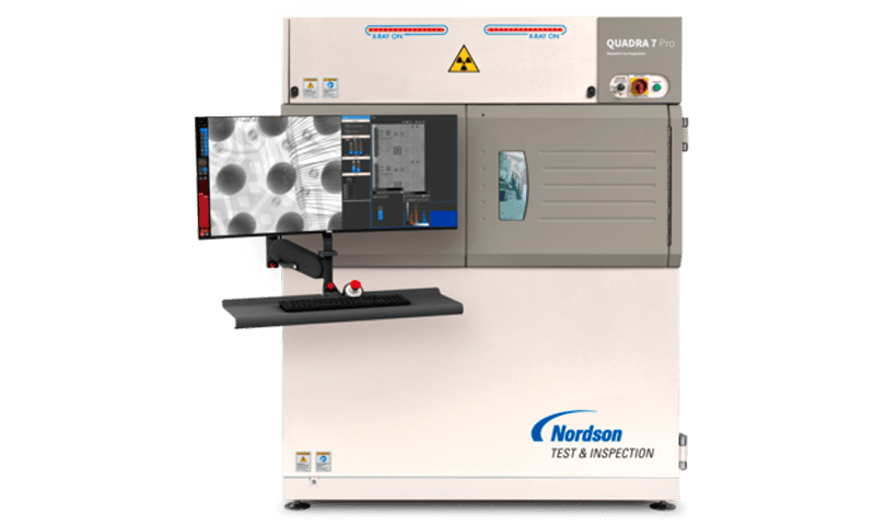
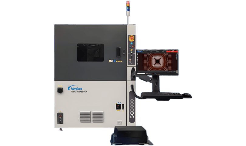
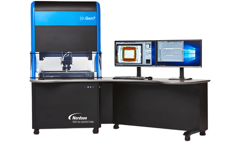
Jeenoce SAM Models Overview
| Model Type | Ideal Use | Key Features |
|---|---|---|
| Entry-Level Benchtop | R&D, small labs, occasional use | Modular frequencies, immersion/tankless options, easy setup |
| Advanced Inline Systems | High-volume SMT lines, inline QC | High-frequency transducers, API for automation, real-time 3D imaging, AI defect detection |
Quick Checklist Before You Buy
Do your samples fit physically inside the system?
Will scan speed meet your line’s throughput needs?
Is the software user-friendly and compatible with your workflow?
Does the model support automation if you plan to expand?
Can you access local or remote support for hassle-free maintenance?
Choosing the right Jeenoce Scanning Acoustic Microscope means balancing resolution, speed, and integration. Our systems are built to grow with your smart factory’s demands, from bench tests to fully automated SMT lines.
Getting started with Scanning Acoustic Microscopy (SAM) doesn’t have to be complicated. Here’s a quick guide to ensure smooth setup and reliable results:
Setup Tips: Coupling Media and Calibration
Choose the right coupling media (usually water or gel) to ensure clear acoustic wave transmission between the transducer and your sample. This reduces signal loss and improves image quality.
Calibrate regularly before scans to maintain accuracy. This includes setting the correct gain, adjusting focus, and verifying timing controls. Calibration keeps your system reliable, especially in production environments.
Troubleshooting Common Issues
Signal noise can show up due to improper coupling or surface roughness. Check for air bubbles and clean your sample and transducer surface.
Artifacts like ghost images or false indications can come from multiple reflections or mounting errors. Adjust scan parameters or reposition samples to minimize these.
Keep a close eye on temperature and environment conditions; these can affect acoustic wave behavior if not controlled.
Training and Certification
Jeenoce offers hands-on operator certification programs designed for both beginners and experienced users. Training covers:
Proper handling and maintenance of SAM hardware
Real-time interpretation of A-Scan, B-Scan, and C-Scan images
Using the software’s AI-assisted defect classification tools
Integrating SAM into your SMT or manufacturing lines
Having certified operators ensures consistent quality control and maximizes your return on investment.
Following these straightforward best practices helps you unlock the full potential of Jeenoce’s Scanning Acoustic Microscopy systems, keeping your production lines running smoothly and detecting defects early.
The future of Scanning Acoustic Microscopy (SAM) is looking exciting, especially with AI-enhanced analysis making defect detection faster and smarter. Using gigahertz frequencies, SAM will push into nanoscale imaging, catching flaws that were once invisible. At Jeenoce, we’re developing hybrid SAM-optical systems that combine the strengths of both methods for even clearer insights.
Sustainability is also a big focus. By reducing waste and improving yield with smarter SAM inspections, smart factories can lower their environmental impact while boosting efficiency. These trends show how acoustic microscopy will stay essential for next-gen smart manufacturing worldwide.
The world's first commercially available ultrasonic scanning microscope was shipped in 1975
Over 20 patented innovations were developed between 1975 and 2005
Our ultrasonic inspection systems represent the standard for quality and accuracy
Our experience in ultrasonic microscopy far surpasses that of other testing providers.

Partnered with the world's top 10 semiconductor companies
Nine of the World's Top 10 Automotive Semiconductor Companies
Seven of the World's Top 10 Defense Contractors
Four of the World's Top 5 MEMS Manufacturers
Seven of the World's Top 10 300mm Wafer Companies
All of the World's Top 5 Semiconductor Storage Chip Manufacturers

We deliver the highest quality images and the most efficient, accurate results
Core components are sourced from our world-leading laboratory specializing in ultrasonic microscopy (ISO/IEC 17025 accredited)
Our patented inspection modes distinguish our equipment from competitors
More than 60 configurable options to suit most products

Our technology optimizes the inspection process, reducing inspection time and improving imaging efficiency
Real-time adjustments to parameters in response to product changes ensure high-precision inspections
In-depth data analysis supports retrospective studies and process optimization
We integrate multiple imaging modes to accommodate diverse testing environments and sample characteristics
Ensure consistent test results across different regions and equipment, maintaining quality standards

As a solution integrator, Jeenoce offers comprehensive, tailored solutions to meet your needs

Message