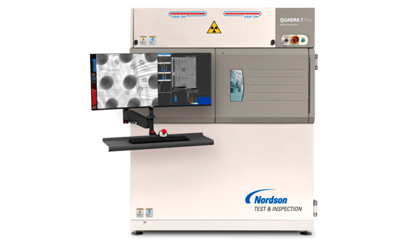
X-ray inspection requirements for semiconductor-grade wafers are more stringent than those for PCBA in standard SMT processing.
This is due to the complex structure and materials of semiconductor products and their critical role as core components in fully assembled devices.
Jeenoce offers X-ray inspection equipment from the world's leading manufacturer to help customers minimize early-stage project losses.
Sample Fixing and Pre-Treatment
Place semiconductor components, such as wafers, chip packages, or complex PCBs, on the inspection table.
Special fixtures may be required for new products at the nanometer level.
Then, remove any factors that may affect the inspection, such as coatings or protective layers.
Equipment commissioning and parameterization
Configure the equipment parameters based on the product's specifications, including power, voltage, detection mode, exposure time, and gain, then prepare to start the inspection.
Data Acquisition Process
Scan the sample using 2D or 3D imaging techniques.
In 3D inspection, thousands of projection images are reconstructed via algorithms into a detailed three-dimensional model of the sample, enabling thorough inspection of internal defects.
Image analysis and reporting
Use algorithms to detect specific defects and generate quantitative data metrics.
Produce targeted inspection reports.
If multiple defects are detected, trace them back to processes such as packaging, soldering, or wafer fabrication.
Adjust process parameters or equipment settings accordingly, and re-inspect to verify improvements.
The operating principle of X-ray inspection equipment, whether for semiconductors, circuit boards, medical, or security applications, relies on X-ray penetration and diffraction characteristics.
Differences in material density and composition allow for the detection of internal structures and defects.
The differences lie in the resolution, voltage, current, and detector sensitivity levels.
In semiconductor nondestructive testing, the focus is on identifying internal microstructural defects and performance issues.
In circuit board testing, the focus is more on line connections and component soldering problems. In contrast, standard security inspections focus primarily on detecting prohibited items. Semiconductor and circuit board tests typically employ both 2D and 3D methods, whereas standard security checks mainly use 2D methods.
Pixel Resolution | 6.5MP |
Feature Resolution | <100nm (at less than 10w) |
Maximum Tube Power | 20w |
Input Voltage | 30-160kv (contact us for personalized solutions) |
Inspection Area | 510 x 445mm (20 x 17.5 inches) (personalized request form inquiry) |
Geometric Magnification | 3000 times (personalized demand form inquiry) |
Total Magnification | 68,000 times (personalized demand form inquiry) |
X-Ray Radiation Leakage | < 1uSv/hr (in accordance with all relevant international standards) |
X-Ray Imaging Software | UK Patents |
For advanced non-destructive testing (NDT) needs, such as planar CT scanning, micron-level 3D modeling, product tracking, or radiation filter trays, contact us for tailored solutions.
In the semiconductor industry, X-ray inspection equipment is used for non-destructive testing.
It scans wafer surfaces and subsurfaces to identify defects such as particles, scratches, or pattern deviations.
It also inspects packaged devices for solder ball voids, package cracks, or bonding wire defects.
In medical and materials science fields, semiconductor X-ray detectors are utilized for high-resolution imaging and spectroscopic analysis, such as crystallographic studies or phase transition analysis.
For example, detectors based on hybrid methylammonium lead iodide (MAPbI3) perovskites excel in synchrotron radiation and medical imaging applications.
Semiconductor X-ray inspection equipment is poised to advance materials, devices, and electronics through upgrades such as larger detectors, faster time response, higher frame rates, and improved energy resolution.
While many manufacturers focus on the price tag, Jeenoce prioritizes your ability to deliver a higher quality product to your customers and the overall benefits throughout the product's lifecycle.
This ensures you can produce high-quality, industry-leading products.
Quality of Image Presentation
Image quality depends on factors such as power, voltage, spot size, detector resolution, and the distance and range of the inspected item.
Select the minimum peak parameters to meet the basic requirements for your most demanding products.
Multi-dimensional inspection requirements
X-ray inspection equipment on the market typically offers 2D, 2.5D (pseudo-3D), and full 3D options.
Lower-dimensional imaging provides less depth information.
For complex product structures, higher-dimensional observation is necessary to ensure optimal yield.
Ease of use for personnel
Is the equipment user-friendly?
Is comprehensive training provided?
These factors are crucial for equipment used in production environments.
If the equipment reduces efficiency or increases defect rates, manual operation may be preferable.
Difficulty of equipment maintenance
Due to the use of X-ray sources, maintenance of these devices differs from standard equipment.
In addition to routine maintenance, special care must be taken for the radiation source.
Key considerations include: ‘Is the radiation level within standard limits? What are the safety procedures for replacing the radiation source?’
These factors must be addressed when considering X-ray inspection equipment.
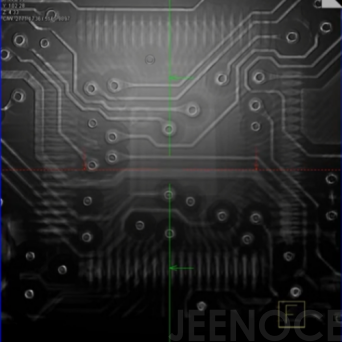
Maximum accuracy of 0.1 micron ensures precise detection of minute details
Our patented dual-mode X-ray source design increases brightness by up to 10 times, making it ideal for semiconductor applications
Our semiconductor experts optimize pixel performance for higher frame rates, lower noise, and clearer images
Display 6.5 MP high-resolution images on a 4K monitor to minimize operator errors
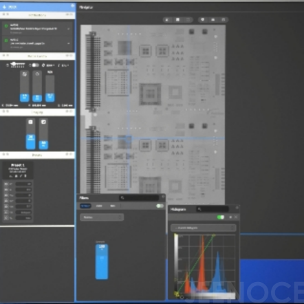
The software offers a customizable interface, enabling users to adjust windows, toolbars, and data panels to suit their inspection needs
The software provides real-time annotation tools (arrows, textboxes, area highlighting) and high-precision measurement functions (distance, area, angle calculations). Users can directly mark defect locations on the image and record their dimensions
Integrated intelligent filtering algorithms (noise reduction, contrast enhancement, edge detection) and multi-modal imaging functions (2D fluoroscopy, 3D tomography) can be used to automatically or manually optimize the imaging effect according to the sample characteristics.
Key functions (start/stop scanning, parameter adjustment, report generation) are integrated into the main toolbar with intuitive icons and shortcut keys, designed for user-friendly operation
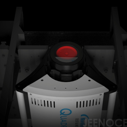
Employs an advanced sealed X-ray tube, delivering high resolution and a long lifespan even at high power
Compared to less reliable X-ray inspection equipment, ours offers superior cost-effectiveness throughout its lifecycle
Double-sealed glass windows prevent radiation leakage
An algorithmic safety mechanism ensures the hatch cannot be operated until it is fully closed
Complies with all national standards for X-ray radiation leakage < 1uSv/hr
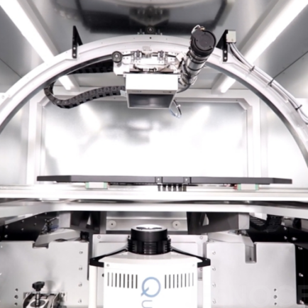
Our world-class manufacturing facility continuously updates the equipment's algorithms based on user feedback
Synchronous upgrades ensure each device benefits from the latest and most advanced detection technology
The new AI technology is being gradually integrated into the device to continuously optimize precision and eliminate error rates
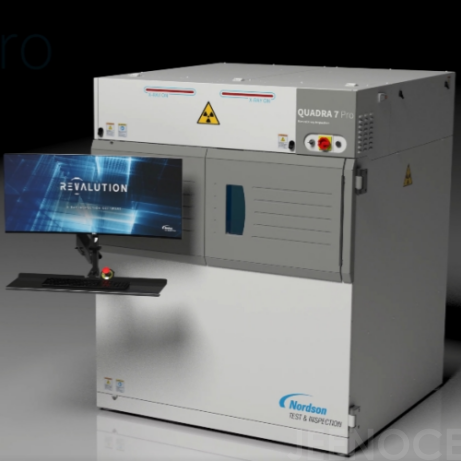
As a solution integrator, Jeenoce provides tailored, one-stop intelligent upgrade solutions

Message
