Reflow soldering is a pivotal process in PCB assembly. It ensures reliable connections in everything from consumer electronics to automotive systems. However, defects can lead to costly failures, reduced product lifespan, and compromised performance.
As a senior engineer with 15 years of experience in Jeenoce, I understand that identifying and resolving these issues is crucial. It ensures high solder joint reliability and optimal manufacturing efficiency.
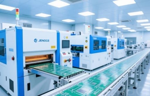
This guide compiles research from ten industry sources and four technical papers. It details around thirty common reflow soldering issues. We’ll explore defects, their causes, and practical solutions to help you achieve flawless PCB assemblies.
Partnering with an experienced provider like JEENOCE is key. They specialize in SMT integration and automation solutions. This partnership helps implement best practices and boost production yield.
Reflow soldering is a key process in surface-mount technology (SMT). Here's how it works:
1.Solder paste is applied to PCB pads.
2.Components are placed onto the paste.
3.The assembly is heated in a controlled oven to melt the solder.
This forms strong electrical and mechanical bonds. The method is essential for high-volume production. It allows precise, automated assembly of complex circuits.
Poor reflow can cause defects like voids in solder joints. These impact thermal and electrical performance.
Proper execution minimizes waste and enhances yield. It also supports the demand for miniaturized, high-density PCBs.
Defects can arise from various factors. These include process parameters, materials, and equipment. Below, we classify the most common issues with brief explanations.
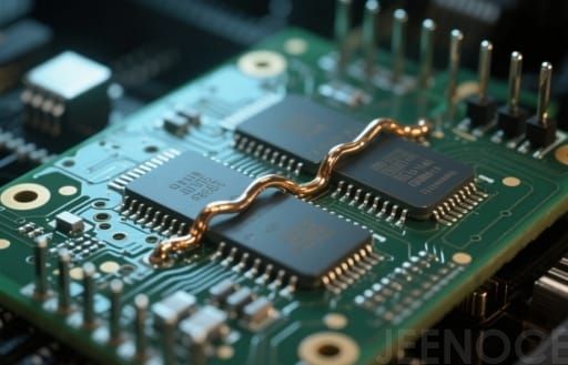
We group defects into categories for clarity:
1.Solder Paste Printing & Application Defects
2.Thermal and Profile-Related Defects
3.Component and Placement Defects
4.Material and Surface Defects
5.Post-Reflow Issues
Each defect includes a description, causes, and impacts on reliability. These are based on standards like IPC J-STD-001.
1.Solder Bridging
Excess solder connects adjacent pads, causing shorts.
Causes: Too much paste, rapid preheat ramp-up.
Impact:Electrical failures.
2.Solder Balls (Solder Beads)
Small solder spheres form around joints.
Causes: Moisture in paste, fast preheat.
Impact: Potential short circuits.
3.Solder Wicking
Solder creeps up the component lead instead of the pad.
Causes: Uneven heating, poor solder mask.
Impact: Weak, incomplete joints.
4.Excessive Solder Joint Fillet
Overly large fillets reduce reliability.
Causes: Too much paste, long time above liquidus (TAL).
Impact: Clearance issues.
5.Insufficient Solder Joints
Small or incomplete connections.
Causes: Low paste volume, poor stencil alignment.
Impact: Weak bonds.
6.Solder Starved Joints
Not enough solder for proper bonding.
Causes: Poor fluidity, short welding time.
Impact: Low mechanical strength.
7.Solder Splashes/Webbing
Irregular solder threads or splashes.
Causes: Rapid heating, unstable temperatures.
Impact: Shorts or aesthetic issues.
8.Solder Beading
Larger balls near components.
Causes: Excess paste, high placement pressure.
Impact: Functional problems.
9.Mid-Chip Solder Balls
Balls under component centers.
Causes: Paste slump, outgassing.
Impact: Poor connections.
10.Solder Skips
Missing solder on pads.
Causes: Uneven pad size, low wave height.
Impact: Open circuits.
1.Tombstoning (Manhattan Effect)
Component lifts on one end.
Causes: Uneven heating, pad mismatch.
Impact: Failed connections.
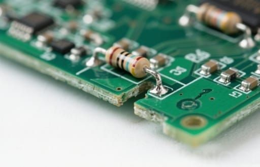
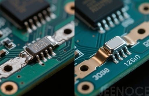
2.Cold Solder Joints
Dull, grainy, incomplete joints.
Causes: Low temperature, short TAL.
Impact: Weak electrical links.
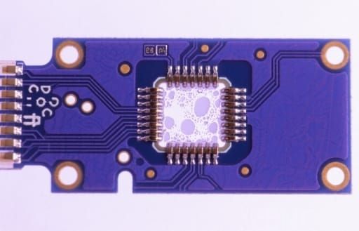
3.Overheating/Thermal Damage
Damage to components or boards.
Causes: High peak temperature, prolonged exposure.
Impact: Delamination or burns.
4.Solder Joint Cracking
Cracks form after reflow.
Causes: Rapid cooling, brittle alloys.
Impact: Reliability failures.
5.Solder Spattering
Solder splatters during reflow.
Causes: Moisture, rapid temperature ramp.
Impact: Particles cause shorts.
6.PCB Warpage
Board bends during reflow.
Causes: Uneven expansion, high temperatures.
Impact: Misalignment.
7.Incomplete Reflow (Under-Reflow)
Solder doesn’t fully melt.
Causes: Low peak temperature, short TAL.
Impact: Grainy, weak joints.
8.Excessive Solder
Rounded, raised joints.
Causes: Late withdrawal, over-application.
Impact: Hidden poor wetting.
9.Solder Joint Discoloration
Discolored joints indicate issues.
Causes: Oxidation, excess heat.
Impact: Reliability concerns.
10.Solder Joint Fatigue
Micro-cracks from stress.
Causes: Improper cooling, CTE mismatch.
Impact: Long-term failures.
1.Component Shift/Misalignment
Parts move during reflow.
Causes: Vibrations, uneven paste.
Impact: Poor connections.
2.Head-in-Pillow (HiP)
Incomplete coalescence in BGAs.
Causes: Oxidation, warpage.
Impact: Open connections.
3. Component Cracking
Cracks in components.
Causes: Thermal shock, moisture.
Impact: Functional failure.
4.Lifted Pads
Pads detach from the PCB.
Causes: Excess heat, mechanical force.
Impact: Fragile boards.
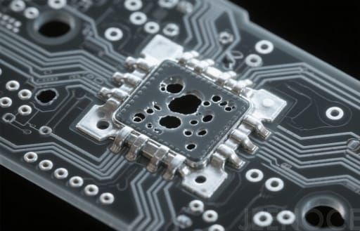
1. Voiding
Gas pockets in joints, like voids in solder joints.
Causes: Outgassing, inadequate profile.
Impact: Reduced strength.
2. Flux Residue
residue left after reflow.
Causes: Excess flux, improper evaporation.
Impact: Corrosion over time.
3. Non-Wetting or Dewetting
Solder doesn’t adhere or retracts.
Causes: Contamination, low flux activity.
Impact: Exposed surfaces.
4. Pin Holes/Blow Holes
Holes in solder joints.
Causes: Trapped moisture, poor plating.
Impact: Conduction issues.
5. Graining (Granular Solder)
Rough, grape-like texture.
Causes: Oxidation, contamination, old paste.
Impact: Weak mechanical and electrical connections.
6.Excessive Intermetallic Compound (IMC) Formation
Thick IMC layers.
Causes: Prolonged high heat, high-tin alloys.
Impact: Brittle joints.
Understanding the root causes of reflow soldering defects is essential for prevention. These factors can be divided into components/materials and process variables.
1.Solder Paste Quality
Poor paste causes voiding, balls, and poor wetting.
Solution: Use low-voiding, high-activity pastes. Store properly (5-10°C).
2. PCB Surface Finish
Bare copper or bad ENIG causes oxidation.
Impact: Weak bonds.
Solution: Use HASL or OSP finishes for better wettability.
3.Component Suitability
Mismatched CTE or moisture leads to cracking.
Solution: Follow IPC standards. Bake moisture-sensitive parts.
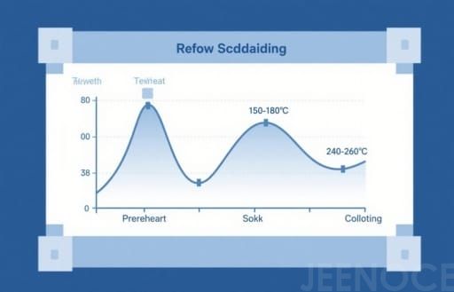
1.Reflow Profile Settings
Wrong settings cause bridging, cold joints, or overheating.
Solution: Follow J-STD-001. Use 1-3°C/sec ramp-up. Soak at 150-180°C for 60-120s. Peak at 240-260°C for lead-free.
2.Temperature Gradients
Uneven heating causes warpage or tombstoning.
Solution: Use nitrogen atmosphere for uniform heating.
3.Atmosphere Control (N2 vs. Air)
Air increases oxidation.
Solution: Use nitrogen to reduce defects by 20-30%.
4.Equipment Calibration
Faulty ovens cause hotspots.
Solution: Regular calibration and thermal profiling.
Improve reliability by optimizing processes and inspections.
Set a proper reflow curve:
Preheat: 150-180°C for 60-120s
Soak: Ensure uniform heating
Reflow: TAL 30-90s
Cool: <6°C/sec
Use thermal profiling best practices:
Attach thermocouples to critical points.
Monitor in real-time.
Adjust for board thickness and component density.
Stencil Design: Use 0.1-0.15mm thickness. Make apertures 10-20% smaller for fine-pitch.
Paste Control: Use automated printers. Optimize squeegee pressure (20-40N) and speed (20-50mm/s).
· AOI (Automated Optical Inspection): Finds surface defects like bridging.
· X-ray Inspection: Detects hidden voids. Aim for <25% per IPC-7095.
· SPI (Solder Paste Inspection): Checks paste volume pre-reflow.
Prevention requires a holistic approach.
Collaborate early with your assembly partner.
Use symmetric pad design for passives to prevent tombstoning.
Add thermal relief on large copper pours to avoid cold joints.
Ensure proper pad spacing to prevent bridging.
Establish a strict maintenance schedule for reflow ovens.
Clean flux residues from fans and ducts.
Verify heater performance and calibrate sensors.
Maintain stencils, squeegees, and placement nozzles.
Train technicians to understand the process.
Help them recognize common defects and perform basic troubleshooting.
Cross-train on SPI, AOI, and X-ray interpretation.
Mitigating reflow issues requires an integrated approach. JEENOCE offers solutions that address these challenges systemically.
We are a technology partner specializing in digital SMT integration and non-standard automation. We work with high-end EMS manufacturers to improve efficiency and yield.
Our core advantages directly address the root causes of soldering defects:
· Turn-key SMT Line Solutions: We provide complete SMT lines with peripheral equipment, ensuring seamless integration to minimize defects like voiding or bridging.
· Self-Developed MES and Digital Factory Systems: Our MES offers component-level traceability, BOM analysis, and real-time data for quick defect detection; the digital factory system supports ERP/MRP for efficient planning and quality control.

· Professional Technical Support and Training: With 10+ R&D engineers and 20+ after-sales staff, we offer comprehensive training. This covers operation, maintenance, and troubleshooting.
· Global Service Network (24/7 Support): We operate in over 50 countries. With 34 after-sales partners, we ensure <2-hour response and <4-hour lead time for key parts.
Addressing reflow soldering problems is vital for robust PCB assemblies. By understanding defects, analyzing causes, and implementing solutions, you can significantly reduce issues.
Partnering with JEENOCE ensures access to cutting-edge SMT solutions. We prevent problems at the source.
Contact JEENOCE today for a free consultation or technical support. Let's optimize your process for maximum efficiency and profits!
Message