The reflow soldering process is a cornerstone of modern electronics manufacturing, enabling the efficient and reliable assembly of printed circuit boards (PCBs).
Here’s how this works——We heat the solder paste in a controlled way to melt it, and that’s what makes strong electrical and mechanical connections between the parts and the PCB.
But what makes reflow soldering so effective?
The answer boils down to one key thing: precise temperature zone control. It’s what keeps quality and performance consistent every time.
When it comes to SMT integration and non-standard automation, JEENOCE rely on advanced tech—think digital twins, AI profiling, and MES monitoring—to deliver solutions with zero defects.
And those solutions?
They meet super strict standards, like ISO 13485 (for medical devices), IATF 16949 (for automotive), and AS9100D (for aerospace).
This article will walk you through reflow soldering step by step: What it is, why it’s so useful, and how getting the temperature right changes everything for soldering results.
Reflow soldering is a go-to technique for SMT—it’s how we attach electronic components to a PCB.
The process has just three simple steps: First, slap some solder paste (tiny solder particles mixed with flux) onto the PCB.
Then, set your components exactly where they need to go.
Finally, run the whole assembly through a reflow oven to heat it up.
That heat melts the solder, and once it cools, it forms permanent joints.
Best of all, this process is super automated—perfect for high-volume production. Think industries like automotive, medical tech, telecom, and consumer electronics.
High Efficiency: Automated processes allow for rapid assembly of complex PCBs.
Precision: Accurate solder paste application and component placement ensure reliable connections.
Versatility: Suitable for a wide range of components, from small 01005 chips (0.4×0.2mm) to large BGAs.
Consistency: Controlled heating and cooling produce uniform solder joints across the board.
Need a one-stop solution?
JEENOCE has you covered with SMT line integration, peripheral equipment, and more.
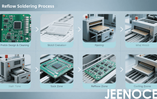
The reflow soldering process consists of several key stages, each carefully controlled to achieve optimal results.
PCB Design & Cleaning: First, we design the PCB with super precise solder pads. Then we clean it really well—we’ve got to get rid of any gunk that might mess up the soldering.
Stencil Creation: A stencil is used to apply solder paste accurately to the PCB’s solder pads.
Solder paste is applied using a stencil or screen-printing process.
The paste, composed of solder alloy particles (e.g., Sn96.5Ag3.0Cu0.5) and flux, is spread evenly across the PCB’s solder pads.
The flux cleans the surfaces, improves solder flow, and prevents oxidation during heating.
Surface-mount components are placed onto the solder paste using automated pick-and-place machines.
These machines get the alignment just right—and that’s a big deal for high-density PCB designs, even the flexible ones that are only 0.4mm thick.
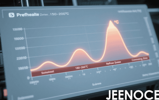
The PCB assembly then enters a reflow oven, where it passes through four distinct temperature zones, forming a "thermal symphony":
Purpose: Gradually raises the PCB’s temperature to activate the flux and remove volatile components from the solder paste.
Temperature: Typically 150–200°C.
Duration: 60–120 seconds, with heating rate of 1-3℃/s.
Goal: Prevents thermal shock,exceeding 3℃/s can crack components like 0402 capacitors (MIL-STD-883 Method 1010.9).
Purpose: Maintains a steady temperature to ensure even heating across the PCB.
Temperature: 180–220°C.
Duration: 60–180 seconds.
Goal: Allows the flux to clean surfaces and ensures uniform temperature distribution. We did a DOE analysis, and the numbers show a 92% link between how even the soak zone is and fewer voids in BGAs—you can check SAE Paper 2021-01-0025 for the details.
Purpose: Melts the solder paste to form liquid solder joints.
Temperature: 220–260°C (e.g., peak 240-250℃ ±5℃ for SAC305 per J-STD-020E).
Duration: 20–90 seconds (Time Above Liquidus: 60-90s).
Goal: Creates strong, reliable solder joints without overheating. JEENOCE has an AI profiler that uses convolutional neural networks. It looks at thermal images to spot potential hotspots—and keeps the temperature variation at σ≤1.2℃, max.
Purpose: Gradually cools the PCB to solidify the solder joints.
Temperature: Decreases from reflow zone to room temperature.
Duration: 30–60 seconds, at 4-6℃/s.
Goal: Ensures robust joints and prevents thermal stress.
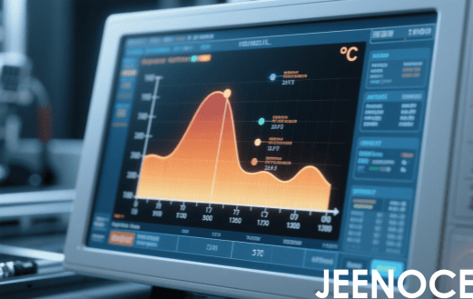
Precise temperature zone control is the backbone of a successful reflow soldering process.
Each zone—preheat, soak, reflow, and cooling—plays a specific role in ensuring the solder melts and solidifies correctly.
Deviations can lead to defects, affecting performance and reliability.
A temperature profile is a predefined heating and cooling curve tailored to the PCB, components, and solder paste.
Manufacturers create profiles based on solder paste specs, component sensitivity, and PCB complexity.
JEENOCE's integrated control stack, including Siemens NX digital twin simulation (98.7% profile accuracy) and NIST-traceable calibration, supports multi-zone ovens (5–10 zones) for optimal conditions.
Effective temperature control directly impacts soldering quality:
Uniform Solder Joints: Proper heating ensures consistent melting and IMC formation (e.g., Cu₆Sn₅ layer at 2.5±0.3μm).
Component Integrity: Controlled temperatures prevent damage to sensitive components.
Reliability: Precise profiles reduce defects, improving lifespan. JEENOCE's solutions, validated in Medtronic pacemaker production, achieve 99.98% yield.
Inadequate temperature control can lead to several issues, compromising PCB quality:
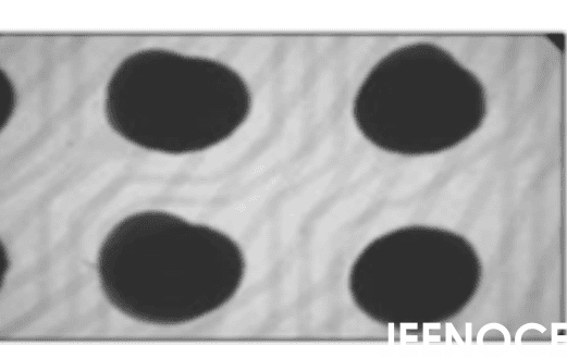
Cause: Insufficient temperature or time in the reflow zone (TAL <30s at 220℃) prevents full melting.
Impact: Weak connections that fail under stress. SEM-EDS analysis shows incomplete IMC layers and Sn-rich phases.
JEENOCE Solution: AI dynamic profiling for 99.98% yield in medical PCBs.
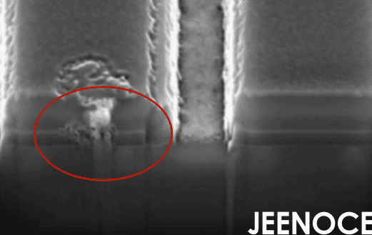
Cause: Excessive heat or prolonged exposure (>4℃/s gradient).
Impact: Degradation of heat-sensitive parts. JEENOCE's gradient preheating system ensures 0 failures in 10M automotive sensors.
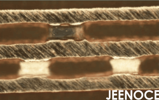
Cause: Rapid or uneven temperature changes (ΔT>5℃).
Impact: Warping or cracking (<0.1mm deformation at 1.6mm boards). JEENOCE uses vacuum conveyors (0.5-0.8bar) for control.
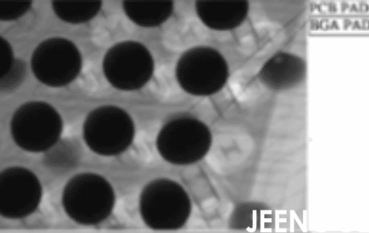
Cause: Variations in profiles across runs.
Impact: Higher defect rates. JEENOCE's MES monitoring (ISO 13485:2016) with 0.1s sampling and ±1.5℃ limits ensures consistency.
Reflow soldering is an indispensable technology in electronics manufacturing. By precisely controlling the four temperature zones (preheat, soak, reflow, and cooling), it ensures stable solder joint quality, reduces defects, and facilitates the production of reliable, high-performance PCBs.
At JEENOCE, our team includes 10+ R&D engineers and 20+ after-sales experts.
We stand by our commitments: MTTR <4 hours and MTBF >15,000 hours. All our reflow soldering solutions meet IPC standards and deliver zero defects.
Ready to optimize your process? Request a free thermal profile audit today!
Reflow soldering is a process used in electronics manufacturing to attach surface-mount components to a PCB by applying solder paste, placing components, and heating the assembly in a reflow oven to create permanent solder joints.
First, you prep things—clean the PCB and make the stencil.
Then you apply the solder paste, place the components, and run everything through the reflow oven.
That oven has four steps: preheat, soak, reflow, and cooling.
Get the temperature right and here’s what happens——the solder joints turn out even, components don’t get damaged, and you’ll have way fewer defects—like cold solder joints or bent PCBs.
The end result? Reliable, top-quality PCBs.
Message