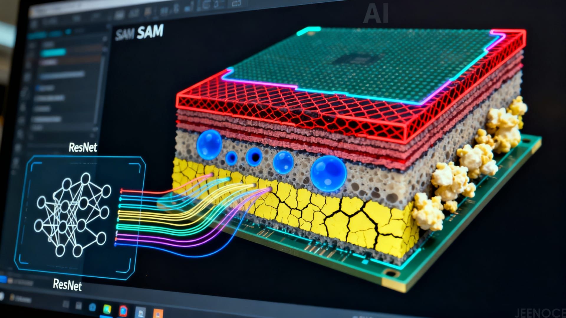
Scanning Acoustic Microscopy (SAM) is a non-destructive testing (NDT) technique that uses high-frequency ultrasonic waves to create detailed images of internal structures in semiconductor packages. By sending sound waves through materials, SAM detects anomalies like voids, cracks, delamination, and other defects invisible to traditional optical or X-ray inspections.
Ultrasonic wave transmission: SAM emits focused ultrasound pulses that reflect differently off material boundaries and defects.
Signal analysis: Reflected waves are converted into high-resolution images revealing internal defects with micrometer precision.
Frequency range: Typically in the 15–100 MHz range, enabling penetration through multiple layers in IC packaging.
Non-destructive flip-chip inspection: Enables thorough internal analysis without damaging costly components.
Delamination analysis in BGA packages: Detects separation between layers or underfill issues critical for reliability.
C-SAM imaging for IC defects: Provides detailed contour maps of voids and cracks in solder joints and underfills.
Popcorn crack identification microscopy: Captures micro-cracks caused by thermal stresses during manufacturing or operation.
SAM excels where optical methods fall short, offering real-time defect detection capable of spotting tiny flaws early in the production line. This early visibility is essential for maximizing semiconductor yield and preventing costly failures downstream.
With demand for higher accuracy and speed, SAM has become a frontline tool in semiconductor packaging inspection. But how can manufacturers move beyond manual SAM imaging to automate defect detection at scale? That’s where the next phase—automation and AI—takes center stage.
Is manual acoustic imaging enough in today’s fast-paced IC manufacturing?

In semiconductor packaging, relying on manual Scanning Acoustic Microscopy (SAM) inspection just doesn’t cut it anymore. Traditional C-SAM imaging for IC defects takes time and depends heavily on skilled operators, making it tough to keep up with fast-paced production lines. That’s where automation steps in.
AI-driven defect recognition changes the game by automating the analysis of acoustic images, spotting issues like delamination in BGA packages, voids in flip-chip assemblies, and popcorn cracks with much greater speed and accuracy. Machine learning models, including ResNet classification of SAM signals, help the system learn complex defect patterns that humans might miss.
This shift to AI-based void detection and real-time defect detection streamlines non-destructive flip-chip inspection and underfill quality control. The results? More consistent defect identification, faster inline defect monitoring on SMT lines, and overall higher throughput. For manufacturers in the U.S. market, this means better yield, reduced waste, and a more scalable quality assurance process that meets today’s demands for efficient, reliable semiconductor packaging.

Jeenoce stepped up by integrating automated scanning acoustic microscopy (SAM) into a busy semiconductor packaging line. Their focus was on speeding up defect detection while keeping accuracy tight, especially for flip-chip and BGA packages where issues like voids and delamination can easily slip through.
Here’s what made their approach work:
Real-time inline defect monitoring directly on the SMT lines, eliminating bottlenecks from manual inspections.
AI-based void detection in flip-chip packaging allowed quick spotting of hidden defects like popcorn cracks or underfill inconsistencies.
The system utilized machine learning in acoustic imaging, specifically ResNet classification models applied to C-SAM signals, improving the recognition of subtle failures.
Deployment in a high-volume environment meant the solution handled thousands of units daily without slowing production down.
By automating non-destructive flip-chip inspection, Jeenoce helped their clients push semiconductor yield higher while cutting costs on rework and scrap. Their smart manufacturing solution shows how AI-driven SAM defect identification works hand-in-hand with real-world production demands.
AI plays a huge role in enhancing Scanning Acoustic Microscopy (SAM) for semiconductor packaging inspection. Instead of relying on manual review, AI-based models analyze C-SAM imaging data quickly and accurately to spot defects like voids, delamination, and cracks.
Here’s how the AI algorithms work with SAM data:
| AI Technique | Role in Defect Identification | Benefits |
|---|---|---|
| Machine Learning (ML) | Learns from large datasets of acoustic images | Fast detection, adapts to new defects |
| Deep Learning (ResNet) | Classifies complex SAM signals, identifies subtle voids and delamination | High accuracy, reduced false positives |
| Automated Voids Detection | Targets voids especially in flip-chip packages | Helps in real-time underfill quality control |
| Pattern Recognition | Detects popcorn cracks and irregularities | Allows early fault prevention |
These AI algorithms convert amplitude and phase data from ultrasonic NDT scans into clear defect maps. The system then flags areas with abnormalities for quick review or automatic action.
By integrating AI-powered SAM, your IC packaging line benefits from:
Real-time defect recognition — no delays in catching issues
Automated underfill and popcorn crack identification — key for BGA and flip-chip reliability
Consistent inline defect monitoring on SMT lines without bottlenecks
The mix of smart AI and advanced acoustic imaging makes SAM a powerful tool for semiconductor manufacturers focused on yield improvement and cost savings. This approach cuts down human error and speeds up semiconductor failure detection, which is crucial for high-volume production environments in the Singapore market.
Automated defect identification using Scanning Acoustic Microscopy (SAM) goes beyond just spotting flaws—it fundamentally drives smarter manufacturing. By integrating AI-powered SAM inspection into semiconductor packaging lines, companies can significantly boost yield. Defects like voids, delamination, and popcorn cracks are detected early, preventing faulty chips from moving down the line and reducing costly rework or scrap.
Here’s how this tech helps:
Yield Optimization: Real-time, non-destructive flip-chip inspection uncovers subtle defects invisible to traditional methods. This early catch translates to higher overall throughput and fewer failures in the field.
Cost Savings: Automated underfill quality control and inline defect monitoring cut labor costs tied to manual inspection. Plus, minimizing waste and rework lowers material expenses and shortens production cycles.
Scalability: AI-driven SAM easily adapts to high-volume IC packaging environments, handling thousands of units without losing accuracy. This scalability aligns perfectly with smart manufacturing goals focused on flexibility and rapid response to changing product demands.
By combining deep learning algorithms like ResNet classification of SAM signals with advanced ultrasonic NDT, manufacturers can confidently ensure quality without slowing down production. This makes automated SAM a key part of semiconductor makers’ toolkit for staying competitive and efficient in today’s fast-paced Southeast Asian market.
Message