If you’re working with advanced packaging like System-in-Package (SiP) or Wafer-Level Packaging (WLP), you already know how tricky low standoff and thermal stress failures can be for your yields. Here’s the deal: conventional reflow methods often struggle to deliver the uniform heat needed to protect tiny solder joints from cracking or warping. That’s where vapor phase soldering (VPS) shines — it’s the precision process that’s redefining reliability by tackling these exact issues head-on. Ready to cut failure rates and boost your packaging quality? Let’s get into why VPS in advanced packaging is becoming the gold standard for eliminating those pain points—and how it fits seamlessly into smart SMT lines.
Are you navigating the complexities of System in Package (SiP) and Wafer-Level Packaging (WLP) for your advanced electronics? These packaging technologies are key to packing more functionality into smaller spaces, but they also come with unique challenges that can impact product reliability.
Advanced packaging moves beyond traditional printed circuit board assembly by integrating multiple components and chips into a compact form. Two popular methods in this arena are:
System in Package (SiP): Combines multiple integrated circuits and passive components into a single package. It’s great for multifunctional, space-constrained applications.
Wafer-Level Packaging (WLP): Packages chips directly at the wafer level, offering thinner profiles and better electrical performance.
Both approaches help boost electronic device performance while reducing size, but the complexity increases the risk of manufacturing issues, especially during soldering.
A significant concern in SiP and WLP is the low-profile solder standoff height. Unlike traditional packages, these solder joints have very minimal space between the component and the substrate. While this low standoff is essential for miniaturization, it poses challenges like:
Reduced mechanical compliance
Increased sensitivity to coplanarity issues
Higher likelihood of solder joint cracking under stress
Low solder standoff can quietly undermine joint integrity, leading to latent failures that are tough to detect early on.
Thermal stress remains a major reliability threat in advanced packaging. The key root causes include:
Coefficient of Thermal Expansion (CTE) mismatch: Different materials expand and contract at varying rates during thermal cycling, putting strain on solder joints.
Thermal fatigue from repeated heating and cooling cycles: Lead-free solder alloys are more prone to crack under prolonged thermal cycling.
Warpage and uneven heating during reflow soldering: Uneven temperatures cause mechanical distortion, weakening the solder connections.
These stress factors contribute directly to solder joint fatigue or fracture, impacting yields and long-term device reliability. Understanding these challenges upfront is critical for selecting the right soldering process that addresses low stand-off and thermal stresses effectively.
Have you encountered stubborn solder joint failures in your SiP or WLP lines? In the next section, we’ll explore why vapor phase soldering offers a precise, game-changing solution to these common problems.

Vapor Phase Soldering (VPS) stands out as a precise and reliable method for achieving uniform reflow, especially in advanced packaging like SiP and WLP. Unlike traditional reflow soldering, VPS uses the condensation of heated vapor to transfer energy evenly, making it ideal for managing low-profile solder standoff heights and reducing common defects.
In VPS, an inert liquid is heated until it vaporizes, creating a stable vapor environment. The components being soldered are exposed to this vapor, which condenses on their surfaces. This condensation transfers heat very evenly and gently, minimizing thermal gradients and avoiding hotspots. The result is consistent solder joints with less chance of warpage or solder joint fatigue caused by CTE mismatch.
VPS allows for precise control over reflow temperature and time, making it possible to optimize reflow profiles specifically for SiP and WLP. This is critical because these advanced packages have tight thermal budgets and unique sensitivity to thermal cycling. Tailoring VPS profiles helps in managing thermal stress failure risks and improving the overall reliability of lead-free solder joints.
Finite Element Analysis (FEA) simulations and rigorous testing back the efficiency of VPS in advanced packaging. These methods confirm that VPS reduces thermal fatigue and solder joint failures often seen in wafer-level packaging with CTE mismatch issues. The uniform heating environment provided by VPS significantly boosts SMT yield improvement and long-term reliability in production lines.
By incorporating VPS, manufacturers can meet the demanding requirements of SiP and WLP while addressing critical issues like warpage control and thermal stress failures effectively.

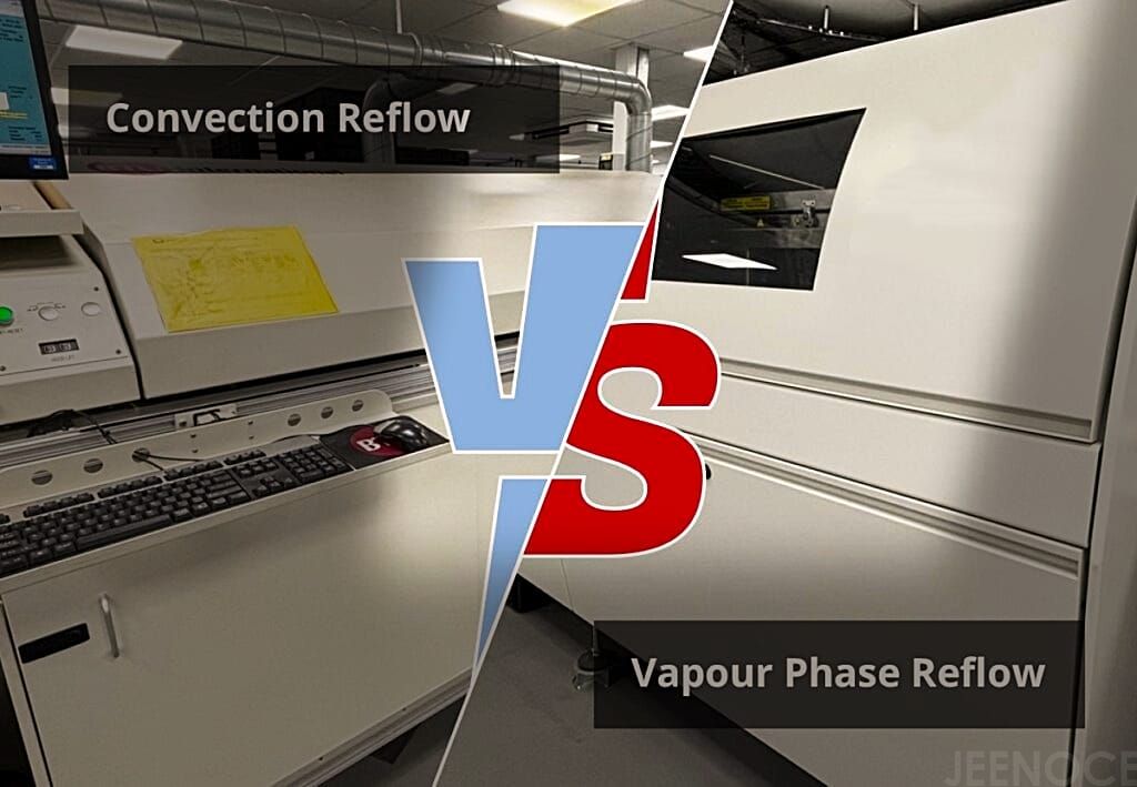
When it comes to tackling thermal stress and ensuring solder joint reliability in advanced packaging like SiP and WLP, vapor phase soldering (VPS) clearly stands out against traditional reflow methods. Here’s why VPS often takes the lead:
Traditional reflow ovens rely on hot air or IR radiation, which can create uneven temperature zones. VPS uses saturated vapor to transfer heat uniformly across the board, reducing hotspots that cause thermal fatigue and warpage.
VPS offers a highly repeatable and stable reflow temperature profile. This precision cuts down on solder joint defects caused by temperature swings—a common issue in low-profile solder standoff joints found in SiP and WLP.
By delivering gentle, consistent heat, VPS better controls advanced packaging warpage and helps manage the coefficient of thermal expansion (CTE) mismatch between materials. This means fewer cracked or brittle solder joints over thermal cycling.
Real-world reports show significant improvement in reliability using VPS:
A major electronics manufacturer reduced thermal stress failures by over 30% after switching from traditional reflow to VPS on wafer-level packages.
Another SiP line saw a noticeable drop in vapor phase reflow defects, leading to higher first-pass SMT yield and improved overall throughput.
VPS enabled consistent, low-profile solder joints that held up better through extended thermal cycling and lead-free soldering processes.
Adopting VPS isn’t without its hurdles. Some common challenges include:
VPS systems may require a higher upfront investment and more floor space. However, the payoff in quality and reduced defects often justifies this.
Fine-tuning VPS profiles for specific SiP and WLP setups takes time but yields a smoother, more reliable reflow process once dialed in.
Operators need proper training on vapor phase technology to avoid mishandling. Starting small with pilot runs helps ease the transition.
Despite these challenges, companies that integrate VPS find it a smart move to improve thermal fatigue resistance, reduce reflow soldering defects, and ultimately boost SMT yield in advanced packaging lines.
Adopting vapor phase soldering (VPS) for SiP and WLP lines can seem challenging at first, but with the right approach and tools, it’s a smooth upgrade. Jeenoce brings smart manufacturing expertise to help with this transition, making the process easier and more efficient.
Assess Your Current SMT Setup
Identify where traditional reflow limits your yield, especially around low standoff heights and thermal stress issues.
Integrate Jeenoce Automation Solutions
Use their customized automation to seamlessly add VPS chambers into your existing SMT lines without major disruptions.
Calibrate VPS Profiles
Tailor reflow temperature and vapor phase profiles specifically for your SiP/WLP packaging parameters, ensuring uniform heating and minimizing defects.
Train Your Team
Focus on proper handling of low-profile solder joints and monitoring vapor condensation stages for consistent quality.
Tracking performance after VPS implementation is key to proving its value:
SPC on Solder Joint Reliability
Monitor defect rates related to low standoff and thermal fatigue for quick feedback.
Yield Improvements
Evaluate throughput and first-pass yield changes after switching to vapor phase reflow.
Energy and Material Savings
VPS often reduces overall energy consumption and rework costs thanks to its precise, uniform heating.
Return on Investment
Calculate reduced warranty claims and improved product lifespan, especially in lead-free soldering environments with tight CTE mismatch concerns.
VPS is not only effective now but designed to scale with the industry:
Vapor phase soldering’s uniform heat transfer is ideal for delicate 3D stacks where thermal stress control is critical.
The precise temperature control in VPS suits advanced solders and substrate materials used in future SiP/WLP designs.
Companies like Jeenoce ensure VPS integrates with Industry 4.0 initiatives, enabling real-time process control and data analytics.
By embedding VPS smartly in your SMT workflow, you’re set to boost reliability, streamline production, and stay ahead as packaging complexity grows.
Message