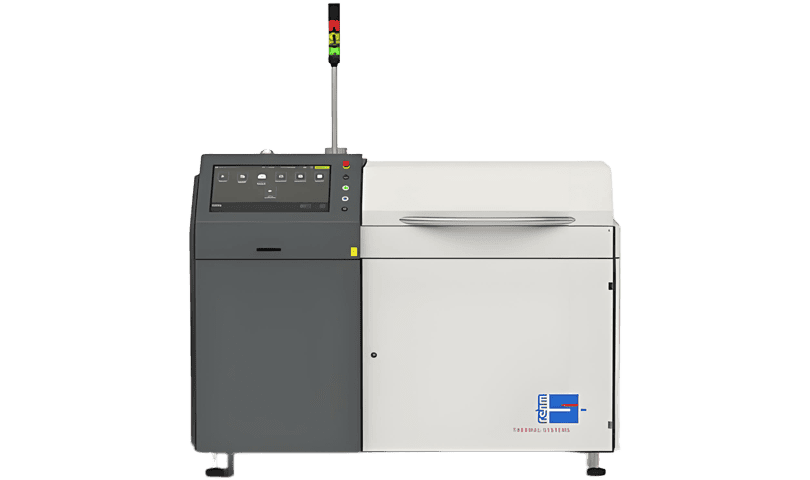
Contact welding(welding) is a kind of welding method for DCB to process substrate mainly (most) semiconductor products in vacuum environment through "teppan firing" process,Jeenoce is positioned as the middle and high-end SMT equipment solution integrator to introduce this equipment mainly to help semiconductor manufacturing customers to accelerate the production pace while producing high yield semiconductor products with the lowest void rate.
It should be noted that the difference between contact welding and pressure welding, formic acid reflow welding,the contact welding equipment adopted by Jeenoce is a special surface heating welding process (or thermal radiation and heat conduction) for the semiconductor industry, rather than pressure welding by mechanical pressing.
Although formic acid can be used to reduce the void rate and remove the surface oxidation problem caused by the welding process,but their processing technology is slightly different because of the different product types.
The purpose of this contact welding(welding) equipment adopted by Jeenoce is to achieve void-free semiconductor products without flux,it is mainly to create a vacuum environment through inert gas, such as 1mbr (please fill in the form for consultation),and the advanced packaging processes and semiconductor wafer welding are completed by precisely controlling the temperature gradient from low to high to low (up to 450°C (450°C requires a form)).
First, the product is placed in a closed welding cavity filled with inert gas, such as nitrogen, N₂/H₂ mixture or 100% hydrogen, and then through the pre-programmed processing process of the parent company's patented control system in Germany, the change of temperature gradient is precisely controlled through the contact heat conduction of the bottom plate surface, and the solder paste is melted.
This step is similar to the process of vacuum reflow soldering.
The difference is that the reflow soldering process is welded by changing the temperature gradient through the transmission device, while the contact soldering process is completed in a closed cavity to output the finished product.
If customer has a high-standard requirements,under the action of high temperature,the decomposition of formic acid into hydrogen and carbon monoxide will reduce with the oxide layer (copper oxide) on the metal surface,which will not only act as a flux, but also prevent secondary oxidation and solder mobility.
Jeenoce's equipment is particularly suitable for welding processes based on DCB substrates, such as IGBT modules etc,however,with the rise of the energy market, the complex structure of wind power system and energy storage device in the new energy industry, especially the battery module of the new energy vehicle, can no longer meet the process standards and quality requirements through simple reflow soldering.
So these markets are also looking for a special process called contact welding.
Besides,it is also suitable for small and medium-sized production scenarios,according to the experience of Jeenoce, small-scale production scenarios are particularly suitable for the laboratory of the military industry.
Producing the highest quality semiconductor products without holes and oxide layer problems
Improving the wetting effect can effectively fill the solder joint and ensure the stability of the circuit connection
Single vacuum chamber complete process greatly improve production efficiency

Maximum heating speed of 150k minutes and maximum cooling rate of 180k minutes enhance the long-term solder joints reliability
Ultra-low vacuum rate is as low as 0.1mba meet the mechanical testing standards of high-standard industries such as aerospace and nuclear power
Peak temperature is 450℃,which is suitable for product in high-power and high-frequency scenarios such as new energy electric vehicle, smart grid and motor drive
Highly sensitive sensors monitor the flow rate,flow volume,filling amount,and temperature of various gases and liquids

Integrated cleaning process removes contaminants in real time and complies with environmental regulations such as RoHS and REACH
Separate cleaning process provides deep cleaning and independent maintenance to reduce the risk of production shutdown
Integrated drying and degassing process can recover heat or exhaust gas for reuse


Message