The rise of X-ray non-destructive testing technology in the field of chip production
Release time:2024-07-05Publisher:Jeenoce
The current testing methods used in semiconductor chip packaging and assembly mainly include manual appearance inspection, flying needle testing, needle bed testing ICT, automatic optical inspection (AOI), and functional testing (functional testing instrument). However, these methods can no longer meet the testing needs of current semiconductor chip packaging processes.
In terms of chip level packaging CSP, there are many types of CSPs, including flexible packaging CSP, rigid substrate CSP, lead frame CSP, grid array lead CSP, and micro CSP. Different CSP structures have different techniques, but they are all based on two techniques: flip chip bonding (FCB) and ball gate array (BGA).
Firstly, there are three connection methods for flip soldering: solder ball protrusion, hot press bonding (and thermal ultrasonic bonding), and conductive adhesive bonding. Regardless of the type of connection convex point, the connection is completely invisible.

Secondly, during the packaging process, solder pads are exposed to air for a long time and are prone to oxidation. Therefore, all connection points may have defects, including cracks in the connecting pads, lack of connection, excessive pad gaps, wire to wire bonding defects, bare chips, and connection interfaces.
In addition, micro cracks may occur during the packaging process of solder pads and silicon wafers due to pressure, and the adhesive connected by conductive adhesive may also produce bubbles during the packaging process. These will all affect the packaging quality of ultra large scale integrated circuits. And invisible defects on the surface, such as convex connections, virtual soldering at connection points, microcracks on silicon wafers, and adhesive bubbles. It cannot be judged by AOI technology. Traditional electrical function testing not only requires a clear understanding of the functionality of the tested object, but also requires high testing skills from testing technicians. The electrical testing equipment is complex and the testing cost is high. The test results depend on the skills of the testers. At the technical level. This has brought new challenges to the packaging and testing of ultra large scale integrated circuits.
Similarly, for SiP packaging systems, two main technologies are used, namely multi chip component technology and 3D packaging. In addition to the inspection issues in 2D packaging mentioned above, due to the complex 3D packaging technology of multi-layer wiring or interlayer stacking and interconnection, 3D quality inspection of SiP chips from bare chips to packaging and printed circuit boards has become more important. Complex AOI technology cannot solve the quality control problem of hidden defects caused by interlayer stacking and multi-layer wiring.
For LED packaging, internal bubbles often appear during chip installation and glue injection, which will affect the quality of the final LED terminal products and bring a series of problems, which is not conducive to the development of China's independent LED products and industry.
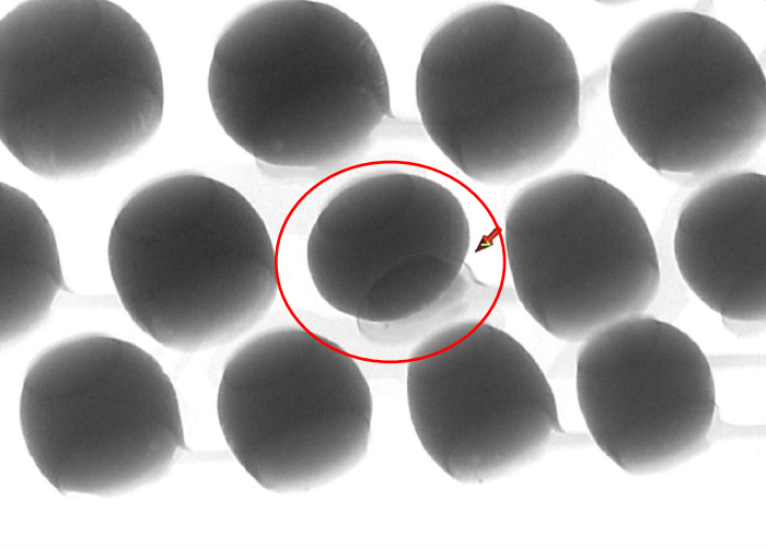
In order to effectively solve the problem of internal defect detection in 2D and 3D packaging, X-ray technology has been used for semiconductor packaging detection, which has more advantages than the above five detection methods. To improve the pass rate and strive for zero defects, a more effective detection method has been provided.
X-ray detection technology uses the absorption differences of X-rays by different materials to image the internal structure of objects, and then performs internal defect detection. It has been widely used in industrial defect detection, medical inspection, and safety inspection fields.

