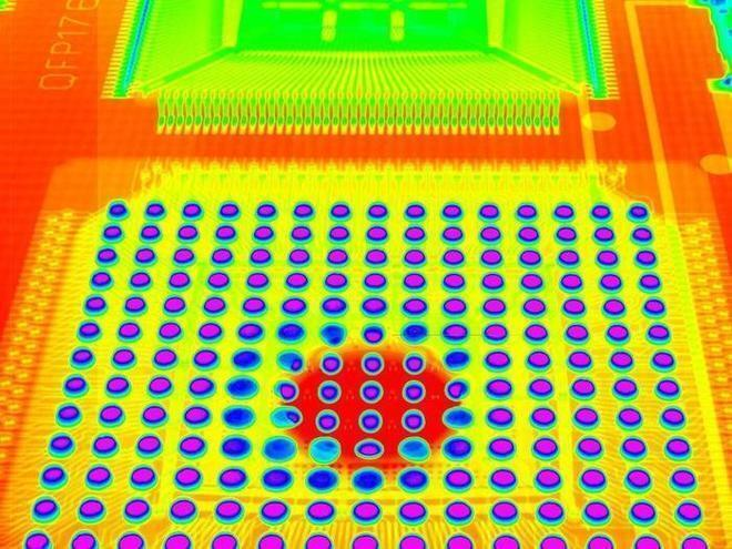
X-ray inspection of BGA solder joint quality for practical application
Release time:2024-07-25Publisher:Jeenoce
BGA is currently a widely used electronic component in the market. Compared with QFP packaged devices or PLCC packaged devices, BGA has a larger number of pins, smaller inductance and capacitance volumes, and more stable heat dissipation performance. Although it has multiple advantages, there are still some obvious shortcomings. For example, after BGA is soldered, all the solder joints are located under the body belly, which cannot be completed by traditional visual inspection, appearance inspection or AOI. Currently, only X-RAY testing equipment can be used to complete the relevant testing operations.

The X-ray device is based on an X-ray source to irradiate the sample. Due to the strong penetration power of X-rays, they can penetrate the product. Then, based on the different light absorption of different materials, the intensity of the light passing through the sample varies. A detector is installed at the top to receive the light and leave images with different brightness.
The main defects detected by BGA are generally concentrated in:
1. Solder bridging can easily cause circuit short circuits;
2. Voids and bubbles in solder joints can easily cause weak connections and poor contact between PCB components during later use;
3. Virtual soldering, which can easily cause device detachment and poor electrical contact;

