Application of X-RAY in detecting the void rate of BGA solder joints
Release time:2024-07-15Publisher:Jeenoce
In the field of electronic product manufacturing, the issue of solder joint voids has always been a concern. Solder joint voids not only affect the mechanical strength and reliability of solder joints, but may also lead to product failures during use. Therefore, effective detection and control of solder joint voids are crucial. X-RAY testing technology, as an advanced non-destructive testing method, plays an important role in detecting solder joint voids.
Firstly, we need to understand the causes of solder joint voids. The main source of solder joint voids is the gas generated by organic substances such as moisture and flux in the material during the welding process at high temperatures. These gases were not effectively expelled before the formation of the solder joint and were trapped in the alloy powder, resulting in the formation of voids. Voids may occur at different levels of the solder joint, including the component layer, pad layer, and solder ball intermediate layer, which can have a negative impact on the connection performance of the solder joint.

X-RAY detection technology has unique advantages in addressing the issue of solder joint voids. X-RAY can penetrate the interior of the package and directly observe the solder joint structure, thereby discovering potential void problems. Compared with traditional destructive detection methods, X-RAY detection has the characteristics of non-destructive, high efficiency, and high accuracy.
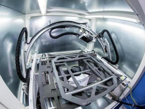
In addition, X-RAY testing equipment is easy to operate and can achieve automated testing on the production line, improving production efficiency. During the process of detecting solder joint voids, the X-ray detection equipment emits X-rays that penetrate the solder joint structure, capturing the reflected radiation information and generating a three-dimensional image of the interior of the solder joint. These images can clearly display the voids inside the solder joints, including their size, location, and distribution. By comparing and analyzing these images, the severity of solder joint voids can be determined, and corresponding measures can be taken for repair or improvement.
In addition to detecting solder joint voids, X-RAY detection technology also has a wide range of applications in other areas. For example, it can be used to detect cracks, fractures, and other physical defects during the packaging process. These defects may stem from factors such as temperature changes, physical pressure, or material mismatches during the packaging process. Through X-ray inspection, these potential issues can be detected in a timely manner to ensure the quality and reliability of the product.
In addition, X-RAY detection can also be applied to nanoscale packaging inspection. With the continuous reduction of semiconductor packaging size, the detection of small defects has become increasingly important. The X-RAY detection equipment, with its high resolution and penetration capability, can achieve precise detection of nanoscale packaging, ensuring product performance and quality. X-RAY testing also plays an important role in internal wiring and copper pillar detection.

