Discussion on the role of X-RAY in BGA detection
Release time:2024-05-20Publisher:Jeenoce
China's electronic technology is developing rapidly, with electronic PCBA processing and packaging showing a trend of high-precision new miniaturization. The quality requirements for circuit assembly such as SMT surface mount processing and plug-in processing are becoming increasingly high. Therefore, higher specification requirements are put forward for testing methods and technologies. To meet the requirements, new detection technologies are constantly innovating, and the application of X-Ray detection technology is one of the best. It can not only detect invisible solder joints, such as BGA, but also qualitatively and quantitatively analyze the detection results, in order to detect faults early.

In the field of electronic manufacturing, common problems mainly include poor BGA infiltration, internal cracks, voids, solder joints, and insufficient solder in ball and sand array devices, faulty parts, misalignment, and hidden components in complex precision assembly components, PCB open/short circuits, and electronic component failures. These questions, with the help of X-ray detection technology, can provide perfect answers to the characterization of the internal physical structure, defect detection and analysis, and failure analysis of semiconductor packaging devices, meeting the testing needs of high-end electronic manufacturing technology, helping to improve manufacturing processes, and greatly increasing yield.
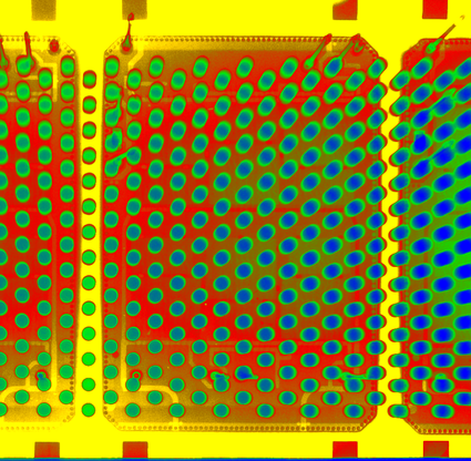
After the BGA device is soldered, all of its solder joints are covered by the device body, so traditional visual inspection methods cannot be used to observe and inspect the welding quality of all solder joints, nor can automatic optical inspection equipment be used to evaluate the appearance of solder joints. To achieve effective detection, X-ray detection equipment can be used to inspect the solder joints of BGA devices.
The main solder joint defects in BGA devices include solder bridging, solder beads, holes, misalignment, open circuit, loss of solder balls, rupture of solder joints, and virtual soldering. These hidden internal defects ultimately have an immeasurable impact on the lifespan and reliability of electronic devices.
With the development of new technologies, ultra-high resolution and intelligent X-ray inspection equipment will not only provide time-saving, labor-saving, and reliable guarantees for BGA device assembly, but also play an important role in electronic product fault analysis, improving fault diagnosis efficiency.

