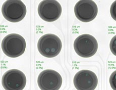
X-ray detection of IGBT semiconductor bubble defects
Release time:2024-04-18Publisher:Jeenoce
IGBT semiconductor is one of the most common components in electronic components, which is packaged by bridging IGBT and FWD through specific circuits. It has the characteristics of low frequency and high power, and has been widely used in various industries, such as inverters, frequency converters, electrolytic power supplies, ultrasonic induction heating, digital electronics, etc. IGBT semiconductor is indispensable. In addition, IGBT semiconductor has the advantage of energy conservation and stability, and can play a core device for energy transmission and conversion.

At present, IGBT semiconductors have not only been introduced in the civilian sector, but also in the national strategic industrial layout system, such as rail transit, smart grid construction, aerospace and new energy industries. In order to better respond to industrial development, the quality of IGBT semiconductors has also become a focus of market attention. The use of X-ray testing as a mainstream detection method for semiconductor bubble defects is currently the mainstream detection method in the market. Its powerful penetrability can effectively and quickly penetrate the internal structure of products. By analyzing the internal structural characteristics of products, the location and size of product defects can be quickly identified.

