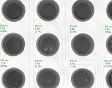
Test of X-ray detection equipment for BGA chip soldering analysis effect
Release time:2024-02-26Publisher:Jeenoce
In recent years, the use of BGA devices in the electronic market has become increasingly widespread. Compared with QFP or PLCC packaging devices, BGA has the characteristics of a larger number of pins, smaller inductance and capacity between pins, and stronger heat dissipation performance. However, BGA also has shortcomings, such as: after BGA welding is completed, all solder joints are located at the bottom position, and eye inspection or AOI inspection cannot make correct quality judgments, So currently, X-RAY devices are commonly used as detection methods in the market.

X-RAY principle
The X-ray equipment is based on the strong penetration ability of X-rays. The light tube emits X-rays in a high-pressure environment, which can effectively penetrate the object to be tested (the penetration effect on lead blocks and materials with large thickness is not obvious, forming a dark image, while the penetration effect on materials with low density and thin thickness is obvious, forming bright spots). The depth of the image formed by different densities and thicknesses is different, thus achieving the detection of BGA device solder joints, Of course, it can also detect many types of products.
There are several common classifications for using X-RAY to detect BGA defects: solder bridging, solder beads, misalignment, open circuit and loss of solder balls, fracture at welded joints, and virtual soldering;

