Application of Microfocus Industrial CT in Defect Detection of Electronic Components
Release time:2024-06-06Publisher:Jeenoce
The three-dimensional tomographic X-ray detection system, also known as industrial CT, has overcome many problems of traditional two-dimensional X-ray detection systems. It designs a focusing section that separates the horizontal area of the PCB by defocusing the upper and lower planes of the target area. The success of this system lies in its ability to accurately detect welding defects in a very short testing and development time. For most circuit boards, "fixture free" also helps reduce the effort spent on product inspection. For small-sized and complex products, it is best for manufacturers to use a fault X-ray detection system. Although all methods can detect welding points, 3D tomography technology provides a non-destructive testing method that can detect all types of welding quality and obtain valuable information to adjust assembly processes.

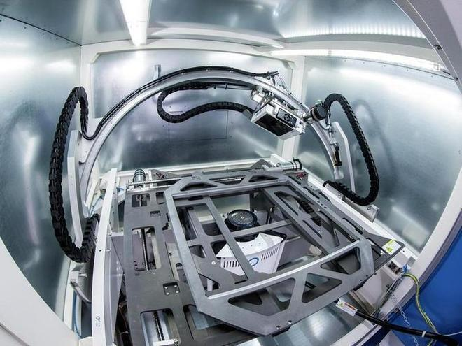
Microfocal industrial CT scanning is the use of X-ray imaging technology to generate multiple two-dimensional images of an object. When the scanned object rotates on the rotating platform, X-rays will penetrate it according to different densities. The radiation that is not absorbed by the parts will be reflected back to the detector panel, generating hundreds of cross-sectional 2D X-ray images, which are then reconstructed to create 3D measurement data.
Throughout the scanning process, there will be no cutting, cutting, stress, pressure, or other forces that may damage or affect the integrity of the parts. The non-destructive features of microfocal industrial CT scanning make it an advanced analysis, quality inspection, and reverse engineering tool for complex geometric shapes and difficult to measure components.
The CT scan results include millions of data points, which can be measured and analyzed to provide some key information. Based on the measurement results, engineers and designers can remove the outer layer, dynamically cut the parts, and observe the discrete distance between the internal parts. The 3D scanning method is provided in the form of a 3D scanning service, which can produce high-quality results with the help of trained technicians.
With the emergence of BGA packaging devices and their large-scale entry into the market, electronic manufacturers need to fully utilize high-tech tools and means to master and vigorously improve the testing technology level in order to control the welding quality of BGA, in response to the characteristics of high packaging density and invisible solder joints. The adoption of new process methods can provide suitable and matching detection methods. Only in this way can quality issues in the production process be controlled. Moreover, the problems reflected during the testing process will be fed back to the production process for resolution, making production smoother and reducing the workload of rework.

