BGA packaging device solder joint defects
Release time:2024-05-16Publisher:Jeenoce
BGA packaging technology has a series of advantages, such as a large number of pins, large I0/terminal spacing (up to 1.00 mm, 1.27 mm, 1.50mm), small inductance and capacitance between leads, enhanced electrical and heat dissipation performance, etc. Therefore, it has developed rapidly and has been applied in products of many international companies (such as IBM, SUN, Fujitsu, Panasonic, MOTOROLA, etc.).

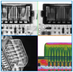
Although the performance of BGA packaged devices has greatly improved compared to other packaged devices, it is difficult to detect solder joint defects because the solder joints of BGA packaged devices are hidden under the device body. In general, manufacturers use visual observation to observe whether the collapse of the outermost solder joint is consistent, and then observe the chip facing the light. If each row and column can pass through light, it can be preliminarily determined that there is no bridging, and sometimes larger solder balls can also be seen. However, using this method to determine whether a solder joint has defects is difficult to satisfy, as it is impossible or difficult to determine whether there are other defects or voids inside the solder joint. To avoid damaging the structure and performance of BGA packaging devices themselves, it is necessary to use other advanced and reliable non-destructive testing methods to identify the inherent defects of BGA packaging devices or to more accurately detect the quality of solder joints. For surface assembly solder joints, the commonly used non-destructive testing method is X-ray inspection. Using an X-ray detector to inspect the solder joints of BGA packaging devices can quickly and accurately detect defects such as bridging, voids, and virtual soldering in the solder joints of BGA packaging devices. It has been widely used in the quality inspection of solder joints in BGA packaging devices.
There are two types of defect detection issues for BGA packaging devices:
(1) Detection of BGA packaged devices themselves. In the production process of BGA packaging devices, it may cause solder ball loss, solder ball too small or too large, solder ball bridging, and solder ball defects. Inspect BGA packaging devices, mainly to check if solder balls are lost or deformed.
(2) Inspection of BGA packaging device assembly solder joints. Mainly inspect the solder joints for bridging, open circuits, insufficient solder, missing balls, porosity, displacement, etc.
With the emergence and large-scale entry of BGA packaging devices into the market, electronic manufacturers need to fully apply high-tech tools and means to control the welding quality of BGAS, and strive to master and improve the level of testing technology. The use of new process methods can have corresponding and matching testing methods. Only in this way can quality issues during the production process be effectively controlled. Moreover, the detection process is reflected in a smoother production process, reducing the workload of rework.

