X-RAY detection technology in circuit assembly
Release time:2024-05-14Publisher:Jeenoce
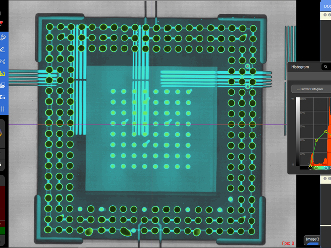
With the rapid development of electronic technology, miniaturization of packaging and high-density assembly, as well as the continuous emergence of various new packaging technologies, the demand for circuit assembly quality is also increasing. So higher requirements were put forward for the methods and techniques of inspection. To meet this requirement, new detection technologies are constantly emerging, and automatic X-ray detection technology is a typical representative of them. It can not only detect invisible solder joints, but also qualitatively and quantitatively analyze the detection results to detect faults early.
There are various testing techniques currently used in the field of electronic assembly testing, including manual visual inspection, flying needle testing, IC needle bed testing, automatic optical testing (AOT), etc. These detection methods have their own advantages and disadvantages:
(1) Artificial visual inspection is a method of examining with the naked eye. Its detection range is limited, and it can only detect missing components, directional polarity, model correctness, bridging, and some virtual soldering. Due to the susceptibility of human subjective and objective factors, manual visual inspection has high instability.
(2) Flying needle testing is a machine inspection method. It uses two probes to power up the device for detection, which can detect defects such as device failure and poor component performance. This testing method is more suitable for plug-in PCBs and PCBs with low density that are mounted with devices of size 0805 or above. However, the miniaturization of devices and the high density of products make the shortcomings of this detection method obvious.
(3) Needle bed testing is a widely used testing technique. Its advantage is fast testing speed, suitable for large quantities of single variety products. However, with the diversification of product varieties, the increase in assembly density, and the shortening of new product development cycles, its limitations have become increasingly apparent.
(4) Automatic Optical Inspection (AOI) detection method. It obtains images of devices or PCBs through CCD photography, and then processes and analyzes them through computers to determine defects and faults. Its advantages are fast detection speed, short programming time, and the ability to be placed in different positions on the production line, making it easy to detect faults and defects in a timely manner, making production, testing, and integration one. It can shorten the time to discover faults and defects, and promptly identify the causes of faults and defects. Therefore, it is currently a widely used detection method. However, the AOI system also has shortcomings, such as inability to detect circuit errors and inability to detect invisible solder joints.

Based on our understanding of various detection technologies and equipment, X-ray detection technology has more advantages compared to the aforementioned detection technologies. It can greatly improve our detection system. To provide us with an effective detection method to improve the "one-time pass rate" and strive for the goal of zero defect E.
The characteristics of X-ray detection technology:
(1) The coverage rate of process defects is as high as 97%. Inspectable defects include: solder joints, bridge connections, standing monuments, insufficient solder, porosity, missing components, and so on. Especially X-ray can be used to inspect solder joint hidden devices such as BGA and GSP.
(2) High testing coverage. It can inspect areas that cannot be detected by naked eye and online testing. For example, if PCBA is judged to be faulty and suspected to be due to a broken wiring in the inner layer of the PCB, X-ray can quickly inspect it.
(3) The preparation time for testing has been greatly reduced.
(4) Defects that cannot be reliably detected by other testing methods can be observed, such as virtual soldering, air holes, and poor molding.
(5) Only one inspection is required for double-sided and multi-layer boards.
(6) Provide relevant measurement information to evaluate the production process. Such as the thickness of solder paste, the amount of solder under the solder joint, etc.

