The difference between X-ray testing and slice testing in PCBA
Release time:2024-01-08Publisher:Jeenoce
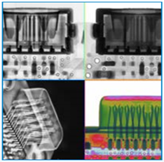
We all know that in PCBA processing, many high-precision circuit boards contain a large number of BGA and IC chips, so the core packaging components cannot visually see the internal welding status on the surface after welding. Therefore, the processing of PCBA requires corresponding detection equipment, and X-ray equipment is the main detection equipment in PCBA detection equipment.
And what kind of testing is slicing done? It is mainly applied to PCB chips, and the quality of PCB chips needs to be tested through this test. If there are significant quality abnormalities in the SMT machine, it is even more necessary to slice and inspect the special parts of the entire soldered circuit board.

Both X-ray testing and slicing testing are internal conditions for soldering circuit boards, but they are targeted at different stages.
X-ray detection application scenarios
1. Observation of internal defects in IC packaging components (such as broken wires, packaging material holes, cracks, etc.);
2. Observe the welding status of the assembled electronic circuit board (such as empty soldering, pilling, bridging, and other abnormal situations);
3. Analysis of porosity ratio in solder joints;
4. Observe various materials from the front, side, and oblique angles;
5. Observe the filling condition of porous materials.
Application scenarios of Cross Section Test
Mainly used for destructive testing of abnormal parts of the sample. Firstly, sample the abnormal parts, then seal and solidify the modified parts with resin, grind and polish them, and finally enlarge and inspect them under a microscope. Compared to the frequency of using X-ray, the probability of using slice detection is very low, and it is not very common for us.

